GF100’s Gaming Architecture
Although it feels like ages ago, NVIDIA announced the Fermi architecture back in September of 2009, focusing on the compute abilities of the GPU that would be GF100. Today’s announcement is about filling in the blanks – where does the graphics hardware fit in to the design that NVIDIA revealed earlier.
As a quick refresher, the GF100 is composed of 512 SPs, which NVIDIA now calls CUDA cores. Each CUDA core is organized in to a block of 32 cores which we call a Streaming Multiprocessor (SM), which in turn are laid out so that 4 of them are in a Graphics Processing Cluster (GPC). Finally, there are 4 GPCs in a single GF100 chip. 32x4x4 = 512 CUDA cores.
| GF100 | GT200x2 (GTX 295) | GT200 (GTX 285) | G92 (9800+ GTX) | |
| Stream Processors | 512 | 2 x 240 | 240 | 128 |
| Texture Address / Filtering | 64/256 | 2 x 80 / 80 | 80 / 80 | 64 / 64 |
| ROPs | 48 | 2x 28 | 32 | 16 |
| Core Clock | ? | 576MHz | 648MHz | 738MHz |
| Shader Clock | ? | 1242MHz | 1476MHz | 1836MHz |
| Memory Clock | ? GDDR5 | 999MHz (1998MHz data rate) GDDR3 | 1242MHz (2484MHz data rate) GDDR3 | 1100MHz (2200MHz data rate) GDDR3 |
| Memory Bus Width | 384-bit | 2 x 448-bit | 512-bit | 256-bit |
| Frame Buffer | ? | 2 x 896MB | 1GB | 512MB |
| Transistor Count | 3B | 2 x 1.4B | 1.4B | 754M |
| Manufacturing Process | TSMC 40nm | TSMC 55nm | TSMC 55nm | TSMC 55nm |
| Price Point | $? | $500 | $400 | $150 - 200 |
When NVIDIA first unveiled GF100, we did not know anything about the ROPs, texture units, or any of the fixed-function graphics units that are customary in a GPU. Today we now have that information, and can discuss where it goes.
While GF100 resembles GT200 in a number of ways as a compute GPU, as a gaming GPU it’s very close to being a complete departure from GT200. The big change here is that the single block of fixed-function hardware as we know it is gone. Virtually every piece of hardware has been split up and moved down a level, and can now be found as part of a GPC or as a SM. NVIDIA’s GF100 block diagram does a good job of showing this.

What’s left of the fixed function hardware is the GigaThread Engine, which is what NVIDIA is calling their scheduler. To understand where our fixed function hardware went, we must meet the newest execution units: The PolyMorph Engine and the Raster Engine.
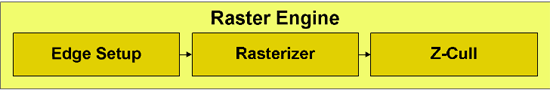
We’ll start with the Raster Engine. The Raster Engine is the combination of all the raster related hardware that we would have found previously in the fixed function pipeline. It does edge/triangle setup, rasterization, and z-culling in a pipelined manner. Each GPC has its own Raster Engine. NVIDIA has very little to say about the Raster Engine, but very little has changed from GT200 besides the fact that there are now 4 of them (one for each GPC) as opposed to 1 larger block. Each rasterizer can do 8 pixels per clock, for a total of 32 pixels per clock over the entirety of GF100.
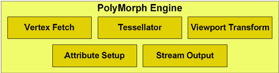
The much more important of the two new execution units is the PolyMorph Engine, which is what NVIDIA is calling the execution unit that handles geometry for GF100. The PolyMorph Engine is responsible for handling Vertex Fetch, Tessellation, Viewport Transform, Attribute Setup, and Stream Output. It’s here where the Tessellator is located, one of the biggest changes that DX11 is bringing to GPU design. Unlike the Raster Engine, each SM has a PolyMorph Engine, giving the GF100 16 PolyMorph Engines altogether.
While the PolyMoprh Engine may sound simple in its description, don’t let it fool you. NVIDIA didn’t just move their geometry hardware to a different place, clone it 15 times, and call it a day. This was previously fixed-function hardware where a single unit sat in a pipeline and did its share of the work. By splitting up the fixed-function pipeline like this, NVIDIA in actuality created a lot of work for themselves. Why? Out of order execution.
OoO is something we usually reserve for CPUs, where high-end CPUs are built to execute instructions out of order in order to extract more performance out of them through instruction level parallelism. OoO is very hard to accomplish, because you can only execute certain instructions ahead of other ones while maintaining the correct result for your data. Execute an add instruction that relies on a previous operation before that’s done, and you have problems. GF100 isn’t a full OoO design, so we’re not going to cover OoO in-depth here, but if you’d like to know more please see this article.
At any rate, internally each PolyMorph Engine is still a simple in-order design. NVIDIA hasn’t gone so far as to make a PolyMorph Engine an OoO design – but because there are 16 of them when there used to be just 1, OoO hazards can occur just as they would in an OoO executing CPU. NVIDIA now has to keep track of what each PolyMorph Engine is doing in respect to the other 15, and put the brakes on any of them that get too far ahead in order to maintain the integrity of results.
To resolve the hazards of OoO, GF100 has a private communication channel just for the PolyMorph Engines that allows them to stay together on a task in spite of being spread apart. The fact of the matter is that all of the work that goes in to making a design like this work correctly is an immense amount of effort, and NVIDIA’s engineers are quite proud of this effort. They have taken the monolithic design of prior GPUs’ geometry units, and made it parallel. We can’t overstate how much of an engineering challenge this is.
However all of this work came at a cost, and not just the significant engineering resources NVIDIA threw at GF100. The other cost was time – we believe that the PolyMorph Engine is the single biggest reason that GF100 didn’t make it out last year. It’s the single biggest redesign of any component in GF100, and is something that NVIDIA had to start virtually from scratch on. When NVIDIA told us that designing a big GPU is hard, this is what they had in mind.
Now why did NVIDIA put themselves through all of this? Because in their eyes, they had to. The use of a fixed-function pipeline in their eyes was a poor choice given the geometric complexity that a tessellator would create, and hence the entire pipeline needed to be rebalanced. By moving to the parallel design of the PolyMorph Engine, NVIDIA’s geometry hardware is no longer bound by any limits of the pipelined fixed-function design (such as bottlenecks in one stage of the pipeline), and for better or for worse, they can scale their geometry and raster abilities with the size of the chip. A smaller GF100 derivative will not have as many PolyMorph or Raster units as GF100, and as a result won’t have the same level of performance; G92 derivatives and AMD’s designs both maintain the same fixed function pipeline through all chips, always offering the same level of performance.

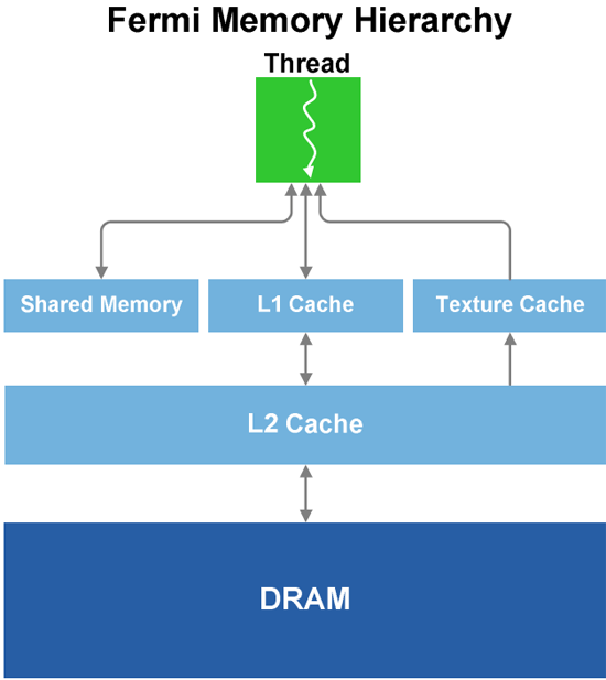
Speaking of performance, we’ll get to that in a bit, but for now we’ll finish our discussion of GF100’s graphics units. Each SM has 4 texture units, which have changes somewhat from the GT200. In GT200, the texture units were at the TPC level; here they are per SM. The texture units are also affected by the cache reorganization of GF100; for L1 cache they still have the same 12KB of texture cache per set of 4 texture units, while they all share GF100’s 768KB L2 cache, which is now used by all execution units and not just textures. Each unit can compute 1 texture address and fetch 4 texture samples per clock, a significantly higher texture fetch rate than on the GT200. Furthermore in conjunction with DX11, NVIDIA’s texture units now support DX11’s new compressed texture formats. Finally, texture units are now tied to the shader clock and not the core clock. They run at 1/2 the shader clock speed of GF100.
Last but not least, this brings us to the ROPs. The ROPs have been reorganized, there are now 48 of them in 6 parttions of 8, and a 64bit memory channel serving each partition. The ROPs now share the L2 cache with the rest of GF100, while under GT200 they had their own L2 cache. Each ROP can do 1 regular 32bit pixel per clock, 1 FP16 pixel over 2 clocks, or 1 FP32 pixel over 4 clocks, giving the GF100 the ability to retire 48 regular pixels per clock. The ROPs are clocked together with the L2 cache.
That leaves us on a final note: clocks. The core clock has been virtually done away with on GF100, as almost every unit now operates at or on a fraction of the shader clock. Only the ROPs and L2 cache operate on a different clock, which is best described as what’s left of the core clock. The shader clock now drives the majority of the chip, including the shaders, the texture units, and the new PolyMorph and Raster Engines. Specifically, the texture units, PolyMorph Engine, and Raster Engine all run at 1/2 shader clock (which NVIDIA is tentatively calling the "GPC Clock"), while the L1 cache and the shaders themselves run at the full shader clock. Don’t be surprised if GF100 overclocking is different from GT200 overclocking as a result.


115 Comments
View All Comments
dentatus - Monday, January 18, 2010 - link
" Im sure ATi could pull out the biggest, most expensive, hottest and fastest card in the world"- they have, its called the radeon HD5970.Really, in my Australia, the ATI DX11 hardware represents nothing close to value. The "biggest, most expensive, hottest and fastest card in the world" a.k.a HD5970 weighs in at a ridiculous AUD 1150. In the meantime the HD5850 jumped up from AUD 350 to AUD 450 on average here.
The "smaller, more affordable, better value" line I was used to associating with ATI went out the window the minute their hardware didn't have to compete with nVidia DX11 hardware.
Really, I'm not buying any new hardware until there's some viable alternatives at the top and some competition to burst ATI's pricing bubble. That's why it'd be good to see GF100 make a "G80" impression.
mcnabney - Monday, January 18, 2010 - link
You have no idea what a market economy is.If demand outstrips supply prices WILL go up. They have to.
nafhan - Monday, January 18, 2010 - link
It's mentioned in the article, but nvidia being late to market is why prices on ATI's cards are high. Based on transistor count, etc. There's plenty of room for ATI to drop prices once they have some competition.Griswold - Wednesday, January 20, 2010 - link
And thats where the article is dead wrong. For the most part, the ridiculous prices were dictated by low supply vs. high demand. Now, we finally arrived at decent supply vs. high demand and prices are dropping. The next stage may be good supply vs normal demand. That, and no second earlier, is when AMD themselves could willingly start price gouging due to no competition.However, the situation will be like this long after Thermi launched for the simple reason, that there is no reason to believe that Thermi wont have yield issues for quite some time after they have been sorted out for AMD - its the size of chipzilla that will give it a rough time for the first couple of months, regardless of its capabilities.
chizow - Monday, January 18, 2010 - link
I'm sure ATI would've if they could've instead of settling for 2nd place most of the past 3 years, but GF100 isn't just about the performance crown, its clearly setting the table for future variants based on its design changes for a broader target audience (think G92).bupkus - Monday, January 18, 2010 - link
So why does NVIDIA want so much geometry performance? Because with tessellation, it allows them to take the same assets from the same games as AMD and generate something that will look better. With more geometry power, NVIDIA can use tessellation and displacement mapping to generate more complex characters, objects, and scenery than AMD can at the same level of performance. And this is why NVIDIA has 16 PolyMorph Engines and 4 Raster Engines, because they need a lot of hardware to generate and process that much geometry.Are you saying that ATI's viability and funding resources for R&D are not supported by the majority of sales which traditionally fall into the lower priced hardware which btw requires smaller and cheaper GPUs?
Targon - Wednesday, January 20, 2010 - link
Why do people not understand that with a six month lead in the DX11 arena, AMD/ATI will be able to come out with a refresh card that could easily exceed what Fermi ends up being? Remember, AMD has been dealing with the TSMC issues for longer, and by the time Fermi comes out, the production problems SHOULD be done. Now, how long do you think it will take to work the kinks out of Fermi? How about product availability(something AMD has been dealing with for the past few months). Just because a product is released does NOT mean you will be able to find it for sale.The refresh from AMD could also mean that in addition to a faster part, it will also be cheaper. So while the 5870 is selling for $400 today, it may be down to $300 by the time Fermi is finally available for sale, with the refresh part(same performance as Fermi) available for $400. Hmmm, same performance for $100 less, and with no games available to take advantage of any improved image quality of Fermi, you see a better deal with the AMD part. We also don't know what the performance will be from the refresh from AMD, so a lot of this needs to take a wait and see approach.
We have also seen that Fermi is CLEARLY not even available for some leaked information on the performance, which implies that it may be six MORE months before the card is really ready. Showing a demo isn't the same as letting reviewers tinker with the part themselves. Really, if it will be available for purchase in March, then shouldn't it be ready NOW, since it will take weeks to go from ready to shipping(packaging and such)?
AMD is winning this round, and they will be in the position where developers will have been using their cards for development since NVIDIA clearly can't. AMD will also be able to make SURE that their cards are the dominant DX11 cards as a result.
chizow - Monday, January 18, 2010 - link
@bupkus, no, but I can see a monster strawman coming from a mile away.Calin - Monday, January 18, 2010 - link
"Because with tessellation, it allows them to take the same assets from the same games as AMD and generate something that will look better"No it won't.
If the game will ship with the "high resolution" displacement mappings, NVidia could make use of them (and AMD might not, because of the geometry power involved). If the game won't ship with the "high resolution" displacement maps to use for tesselation, then NVidia will only have a lot of geometry power going to waste, and the same graphical quality as AMD is having.
Remember that in big graphic game engines, there are multiple "video paths" for multiple GPU's - DirectX 8, DirectX 9, DirectX 10, and NVidia and AMD both have optimised execution paths.