AMD Core Counts and Bulldozer: Preparing for an APU World
by Anand Lal Shimpi on November 30, 2009 12:00 AM EST- Posted in
- CPUs
Last week Johan posted his thoughts from an server/HPC standpoint on AMD's roadmap. Much of my analysis was limited to desktop/mobile, so if you're making million dollar server decisions then his article is better suited for your needs.
He also unveiled a couple of details about AMD's Bulldozer architecture that I thought I'd call out in greater detail. Johan has been working on a CMP vs. SMT article so I'll try to not step on his toes too much here.
It all started about two weeks ago when I got a request from AMD to have a quick conference call about Bulldozer. I get these sorts of calls for one of two reasons. Either:
1) I did something wrong, or
2) Intel did something wrong.
This time it was the former. I hate when it's the former.
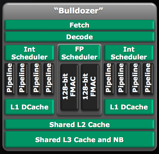
It's called a Module
This is the Bulldozer building block, what AMD is calling a Bulldozer Module:
AMD refers to the module as being two tightly coupled cores, which starts the path of confusing terminology. A few of you wondered how AMD was going to be counting cores in the Bulldozer era; I took your question to AMD via email:
Also, just to confirm, when your roadmap refers to 4 bulldozer cores that is four of these cores:
http://images.anandtech.com/reviews/cpu/amd/FAD2009/2/bulldozer.jpg
Or does each one of those cores count as two? I think it's the former but I just wanted to confirm.
AMD responded:
Anand,
Think of each twin Integer core Bulldozer module as a single unit, so correct.
I took that to mean that my assumption was correct and 4 Bulldozer cores meant 4 Bulldozer modules. It turns out there was a miscommunication and I was wrong. Sorry about that :)
Inside the Bulldozer Module
There are two independent integer cores on a single Bulldozer module. Each one has its own L1 instruction and data cache (thanks Johan), as well as scheduling/reordering logic. AMD is also careful to mention that the integer throughput of one of these integer cores is greater than that of the Phenom II's integer units.
Intel's Core architecture uses a unified scheduler fielding all instructions, whether integer or floating point. AMD's architecture uses independent integer and floating point schedulers. While Bulldozer doubles up on the integer schedulers, there's only a single floating point scheduler in the design.
Behind the FP scheduler are two 128-bit wide FMACs. AMD says that each thread dispatched to the core can take one of the 128-bit FMACs or, if one thread is purely integer, the other can use all of the FP execution resources to itself.
AMD believes that 80%+ of all normal server workloads are purely integer operations. On top of that, the additional integer core on each Bulldozer module doesn't cost much die area. If you took a four module (eight core) Bulldozer CPU and stripped out the additional integer core from each module you would end up with a die that was 95% of the size of the original CPU. The combination of the two made AMD's design decision simple.AMD has come back to us with a clarification: the 5% figure was incorrect. AMD is now stating that the additional core in Bulldozer requires approximately an additional 50% die area. That's less than a complete doubling of die size for two cores, but still much more than something like Hyper Threading.


94 Comments
View All Comments
Alberto - Tuesday, December 1, 2009 - link
You are right.The eight core Sandy Bridge will have over 200 Gflops Double Precision with a power budget of 130W in 32nm and 95W in 22nm.
In these conditions the "dream" to throw away the Fp unit from the CPU it's only a Nvidia desire.....to survive.
gruffi - Sunday, December 6, 2009 - link
Give me your calculation please. I see Sandy Bridge nowhere near 200 GFLOPS in DP.Sandy Bridge may have up to 8 cores/16 threads (the known die shot shows only 4 cores), probably clocked around 3 GHz.
4 DP (AVX/256-bit) * 1 op/cycle (no FMA) * 8 cores * 3 GHz = 96 GFLOPS
OTOH, AMD may have twice as much FP throughput with "Interlagos" (8 modules/16 cores/16 threads) if we assume similar clock rates.
4 DP (AVX/256-bit) * 2 ops/cycle (FMA4) * 8 modules * 3 GHz = 192 GFLOPS
psychobriggsy - Tuesday, December 1, 2009 - link
That certainly beats AMD's ~100GFLOPS in double precision from an 8-core Bulldozer.Calculation: 3GHz * 2 (FMA) * 2 (units) * 2 DP (128-bit unit) * 4 (modules).
Clearly AMD are providing enough CPU power for OpenCL, etc, to run "well", but if you need "serious" power then you'll plug in an RV900 series GPU that will probably try to get near 1TFLOP in DP in the same timeframe. With OpenCL, the exact same code will run (AMD's OpenCL driver can switch between CPU and GPU without any application changes).
epobirs - Tuesday, December 1, 2009 - link
It looks like AMD is engaging in another word of words instead of performance. Remember when they claimed ownership of what was or was not 'dual core' and 'quad core?' While AMD declared the C2Q line as 'not true quad-core' the Intel product was actually shipping and available for use a year before AMD's 'true' chips came out with less performance and some serious bugs for added enjoyment.This gets tiresome to the point where I hold AMD in great suspicion when they lead with a new official vocabulary instead of the product and how it actually performs.
I truly don't give a damn about your modules, AMD. Take your new architecture and define the smallest portion that could be sold as a discrete product to run a PC. That is a core. It doesn't matter how many threads it runs. It is a core. If we cannot have meaningful definition to which all companies adhere, the conversation is dead and all that remains is useless PR blather.
Nehemoth - Tuesday, December 1, 2009 - link
Well said. At the end of the day users don't care about the elegance of the architecture they'll care about performance, performance per watt, etc, etc.PD : Where is the Z Ram technology they're licensed back time ago for the Cache Memory?
What about the license for XDR from Rambus?
At less for some servers should have a value.
Milleman - Monday, November 30, 2009 - link
It's good to see that the existance of AMD is healthy for the competition, progress and innovation. The existance of AMD is even good for the Intel fan-boys. The Inte CPU's wouldent be half that fast today, if there wasn't any competition on the market.jmurbank - Monday, November 30, 2009 - link
An AMD representative said that the picture you provided is one core, but it has two integer units. These two integer units are hardware basis of a similar feature of Intel's Hyperthreading. The following picture is a dual core.http://images.anandtech.com/reviews/cpu/amd/Bulldo...">http://images.anandtech.com/reviews/cpu/amd/Bulldo...
The four core is the following image.
http://images.anandtech.com/reviews/cpu/amd/Bulldo...">http://images.anandtech.com/reviews/cpu/amd/Bulldo...
This is all assuming the Bulldozer core is for their enthusiasts or high end setups. For the low end, these pictures will not include two integer units. Though it all depends what AMD has in store for the microcode for their Bulldozer core because it can be one way and other or it can be both that can take advantage of both features by including a switch in the BIOS or software, but it is too soon.
Milleman - Monday, November 30, 2009 - link
Looks like the AMD CPU's are slowly getting structures "borrowed" from ATI GPU's, which is very interrresting. The traditional CPU strukture from the seventies are on the way out. The future looks really exciting!tatertot - Monday, November 30, 2009 - link
AMD marketing made a mistake (Fruehe, on his blog) when referring to an AMD engineering claim made by Moore.The claim is on slide 4:
http://www.amd.com.cn/chcn/assets/content_type/Dow...">http://www.amd.com.cn/chcn/assets/conte...loadable...
80% more throughput (integer work) for 50% more (core) area.
Fruehe LOLed this into 80% more performance for 5% more area (ooops!), and now this meme has taken hold.
It's wrong. Each module is 50% larger to get 80% more integer throughput, and even adding in all the "uncore" portions on a chip does not get this number anywhere NEAR 5%. (The uncore is nowhere near 10x the area of all the core area combined)