NVIDIA's Fermi: Architected for Tesla, 3 Billion Transistors in 2010
by Anand Lal Shimpi on September 30, 2009 12:00 AM EST- Posted in
- GPUs
The graph below is one of transistor count, not die size. Inevitably, on the same manufacturing process, a significantly higher transistor count translates into a larger die size. But for the purposes of this article, all I need to show you is a representation of transistor count.
![]()
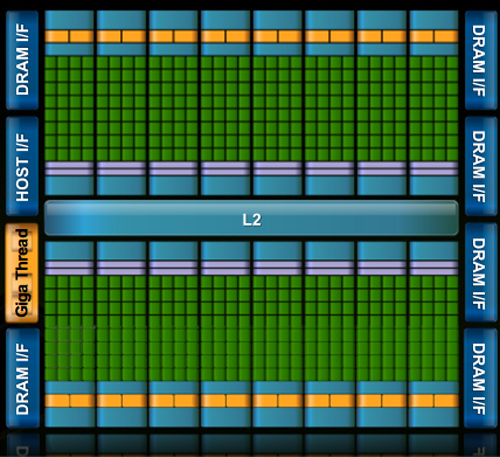
See that big circle on the right? That's Fermi. NVIDIA's next-generation architecture.
NVIDIA astonished us with GT200 tipping the scales at 1.4 billion transistors. Fermi is more than twice that at 3 billion. And literally, that's what Fermi is - more than twice a GT200.
At the high level the specs are simple. Fermi has a 384-bit GDDR5 memory interface and 512 cores. That's more than twice the processing power of GT200 but, just like RV870 (Cypress), it's not twice the memory bandwidth.
The architecture goes much further than that, but NVIDIA believes that AMD has shown its cards (literally) and is very confident that Fermi will be faster. The questions are at what price and when.
The price is a valid concern. Fermi is a 40nm GPU just like RV870 but it has a 40% higher transistor count. Both are built at TSMC, so you can expect that Fermi will cost NVIDIA more to make than ATI's Radeon HD 5870.
Then timing is just as valid, because while Fermi currently exists on paper, it's not a product yet. Fermi is late. Clock speeds, configurations and price points have yet to be finalized. NVIDIA just recently got working chips back and it's going to be at least two months before I see the first samples. Widespread availability won't be until at least Q1 2010.
I asked two people at NVIDIA why Fermi is late; NVIDIA's VP of Product Marketing, Ujesh Desai and NVIDIA's VP of GPU Engineering, Jonah Alben. Ujesh responded: because designing GPUs this big is "fucking hard".
Jonah elaborated, as I will attempt to do here today.


415 Comments
View All Comments
Kougar - Friday, October 2, 2009 - link
Hey Anand:Just wanted to say thanks for the article. Love the quotes and behind-the-scene views, and in general the ever so informative articles like this that just can't be found elsewhere. So, thank you!
bobvodka - Friday, October 2, 2009 - link
Someone earlier askes if supporting doubles was going to waste silicon, I don't think it will.If you look at the through put numbers and the fact that FP64 is half that of FP32 with the SFU disabled I suspect what is going on is that the FP64 calculations are being done by 2 cores at once with the SFU being involved in some way (given how it is decoupled from the cores there is no apprent good reason why the SFU should be disabled during FP64 operation).
A comment was also made re:ECC memory.
I suspect this wont make it to the consumer board; there is no good reason to do so and it would just cost silicon and power for a feature users don't need.
Zool - Friday, October 2, 2009 - link
Maybe the consumer board wont hawe ECC but it will be still in the silicon (disabled). I dont think that they will produce two different silicons just becouse of ECC.bobvodka - Friday, October 2, 2009 - link
hmmm, you are probably right on that score and that might aid yield if they can turn it off as any faults in the ECC areas could be safely ignored.Chances of them using ECC ram on the boards themselves I would have said was zero simply due to cost :)
halcyon - Friday, October 2, 2009 - link
Same foundry, same process, much more transistors....Based on roughly extrapolating scaling from the RV870, how much bigger power draw would this baby have?
The dollar draw from my wallet is going to be really powerful, that's for sure, but how about power?
deeper - Friday, October 2, 2009 - link
Well, not only is the GT300 months away but it looks like the card they showed off is a fake anyhoo, check it out at Charlie Demerjian's www.semiaccurate.comZool - Friday, October 2, 2009 - link
Could you pls delete majority of SiliconDoc replies and than this after them. Its embarassing to read them.Pirks - Friday, October 2, 2009 - link
I call BS. How many people have 2560x1600 30-inchers? Two? Three? Main point - resolutions are _VERY_ far from being stagnated, they have SOOOOOOOOO _MUCH_ room for growth until 2560x1600 which right now covers maybe 1% of the PC gaming market. 90% of PC gamers still use low-res 1680x1050 if not less (I for one have 1400x1050, yeah shame on me, I don't want to spend $800 on hi-end SLI setup just to play Crysis in all its hi-res beauty, for.get.it.)Shame Anand, real shame.
Otherwise top notch quality stuff, as always with Ananad.
bigboxes - Friday, October 2, 2009 - link
1680x1050 = low res??? Seriously? That's hi-def bro. I understand you can do better, but for my 20" widescreen it is definitley hi-def.JarredWalton - Friday, October 2, 2009 - link
I believe what you describe is exactly what is meant by stagnation. From Merriam-Webster: "To become stagnant." Stagnant: "Not advancing or developing." So yeah, I'd say that pretty much sums up display resolutions: they're not advancing.Is that bad? Not necessarily, especially when we have so many applications that do thing based purely on the wonderful pixel instead of on points or DPI. I use a 30" LCD, and I love the extra resolution for working with images, but the text by default tends to be too small. I have to zoom to 150% in a lot of apps (including Firefox/IE) to get what I consider comfortably readable text. I would say that 2560x1600 on a 30" LCD is about as much as I see myself needing for a good, looooong time.