Globalfoundries Starts on 22nm Fab & Announces First non-AMD Customer
by Anand Lal Shimpi on July 29, 2009 4:01 AM EST- Posted in
- CPUs
Somehow I’d managed to dodge meeting with Globalfoundries since the company was formed earlier this year. For those of you who don’t know, AMD is now officially a fabless semiconductor. AMD provided its two existing fabs to the new company and its partner, ATIC (Advanced Technology Investment Company) provided $6B. ATIC owns 65.8% of the new company and AMD owns the rest, although the two share voting rights.
AMD’s biggest limitation has always been capital. Intel currently has four fabs that will be producing 32nm chips by the end of 2010, AMD currently has (err, had) a single 45nm fab in Dresden. There’s simply no way AMD could compete in the fab game with Intel, so it chose to partner up with ATIC, take $6B of their dollars, and spin off its fab business.
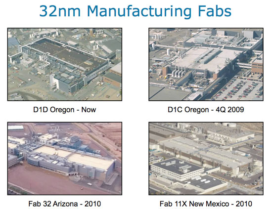
Intel's 32nm fabs for 2010
Until this morning, Globalfoundries only had a single customer - AMD, but that just changed with the announcement that STMicro would be using their fabs. Currently Globalfoundries only has AMD’s two fabs in Dresden, Germany, only one of which is producing modern 45nm SOI wafers. But that too is about to change.

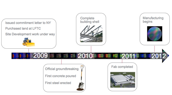
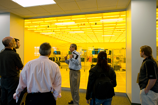
Ceremonial shovels, at a ceremonial ground breaking
My first official meeting with GF came just this past week, in Saratoga County, NY. That’s the site where its brand new post-AMD fab will be constructed and it’s sort of a big deal. I was there for the ceremonial ground breaking, but concrete doesn’t get poured until September, the shell won’t be finished until 2010 and the fab won’t be done until 2011. Globalfoundries won’t be able to ship revenue generating wafers until 2012. But that’s ok, with $6B in the bank and a strong commitment from wealthy ATIC the company couldn’t be in a better place.
On Competing with TSMC
AMD couldn’t last competing in the foundry game with Intel. The chart below just shows how expensive it gets:
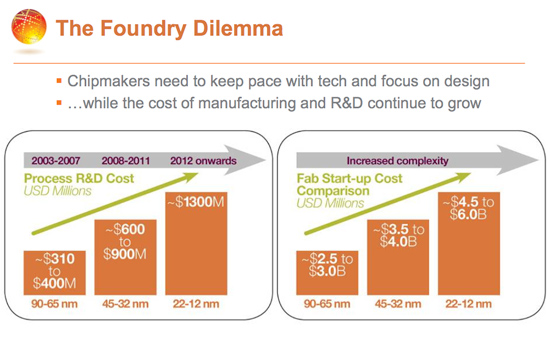
At 32nm a single fab can cost $4B and in just two years it’ll need to be upgraded (to the tune of around a billion) to support 22nm production. For AMD to support the costs alone and remain competitive with Intel, it would have to virtually own the x86 microprocessor market. Even when AMD held the technology crown, that didn’t happen.
The other alternative is to subsidize the cost of these expensive factories over multiple customers. This is where things get interesting. AMD alone may not be able to fill a fab and make the investment pay off, but AMD + Sony + Toshiba + NVIDIA + etc... can definitely make it work.
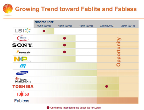
Globalfoundries' potential customers and when they plan on going fabless
Currently, fabless semiconductor manufacturers like NVIDIA (and the graphics division of AMD) go to foundry companies like TSMC for their manufacturing needs. In return, they get nearly the latest manufacturing processes (TSMC is at 55nm for volume and 40nm while Intel is at 45nm moving to 32nm) and don’t have to worry about building expensive fabs.
There are problems with this approach. For starters, TSMC has been having troubles moving to 40nm - as you may have heard. Just as important, you don’t get the most advanced manufacturing process technically available. There’s also the fact that TSMC has very little real competition in the industry; all of the GPUs you’re used to reading about are made at TSMC.
The machine to the left of the man's head in the center of the pic is a 193nm lithography machine. We weren't allowed to take close photos, but that machine costs around $75M. Fabs are expensive.
Companies like Sony, Freescale, Samsung, Toshiba and TI all currently fab their own chips. These chips are far less complex than a Nehalem or a Radeon HD 4890 and are thus made on 130nm, 90nm or 65nm processes. The SoC (System on Chip) in the iPhone 3GS is built on a 65nm process by Samsung at its own fab. Being able to move to 45nm or 32nm alongside Intel would give Apple, Samsung and even ARM in general a tremendous competitive boost in the market place. A 45nm iPhone 3GS would use less power or even run at higher clock speeds.
The need for a modern fab partner increases as you look at Intel’s motions towards competing in the smartphone space. Once Atom finally makes its way into smartphones, Intel could have a manufacturing advantage over the ARM partners - allowing for quicker scaling to lower power and higher performance designs. In other words, companies making smartphone SoCs need a good foundry option to compete with Intel.


50 Comments
View All Comments
iwodo - Wednesday, July 29, 2009 - link
There are loads of questions to be asked, I hope Anand could provide some insight.1. AMD's problem is not having enough fabs to manufacture its chip therefore to keep healthy supply. Considering AMD have had 30% market share before without much help from OEMs. They were doing very good. And discounting ATI 's chip are not even produce from GF. They dont even have enough capacity to keep up with their own products. Why are they signing up other players?
2. The X86 issues - i believe everyone is allowed to design an X86 CPU, but to manufacture it require a license from Intel. Now GF has the license to make X86 for AMD. Doesn't that mean other players could theoretically make x86 CPU ( Nvidia ?? ) Ofcoz, getting X64 from AMD is a different story.
3. What is the current Physical Limit we can downsize to? Since Atom are measured in size of pm ( 1nm = 1000pm ) . I know Intel has an up to 11nm roadmap. If, and if we can get to single digit nm scale then i honestly believe ARM dont have a fighting chance against Intel. Not to mention 3D and Muti Gate tech will help.
4. Any info on how many fabs Intel, Samsung and other players owe?
5. Are fabs for Flash a lot cheaper?
willstoddard - Wednesday, July 29, 2009 - link
I think the limit is not necessarily going to be physical limit as much as a fiscal limit. The photo lithography process is the Fab limiter. It always has been. The Nikon S620 is just beginning to ship to customers (Currently Intel only). It is targeted for the 32nm node. ASML has the XT:1950Hi at the same node. Intel will push these machines beyond advertised specs to produce 22nm gate layers.Both Nikon and ASML have EUV (x-ray) machines in second stage beta. However there are still significant hurtles to overcome. EUV requires exposure under Cryo vacuum pressures. This is new to both companies. X-rays do not penetrate quartz or CaF2 optics, so only mirrors can be used, including the projection lens system. This causes significant amounts of flare. They will work through these and many other issues, but my crystal ball tells me the the biggest hurtle will be making the technology economically viable to IC makers. The cost of one 32nm node lithography immersion scanner is 40+ million dollars. You can negotiate a better deal if you buy more. ASML tends to be ~7 to 10 million more per machine than the comparable Nikon because they have to buy the projection lens from Carl Zeiss. Nikon makes their own. The larger fabs have as many as 40 of these machines. These machines have a throughput of 170 (300mm) wafers per hour (ASML) and 200 WPH (Nikon). The EUV machines will cost $80M+ and will have ~40WPH (300mm) throughput, limited by the illumination source and delivery system.
When the machines cost twice as much and have 1/5th the output capacity, it is difficult to make a viable business model.
So what will happen? I think EUV will still need to mature for another 5-7 years before it is a viable option.
The article states that immersion technology lowers the wavelength of the light as it passes through water. In fact, it does no such thing. It simply changes the refractive index of the medium the light is travelling through from ~1.00 of air to ~1.44 for water. This changes the angle of the light leaving the projection lens and allows higher order diffected rays to reach the wafer surface which increases contrast of the image.
I think we will see other innovations in the current lithography systems that will get us to 12nm. Researchers are looking for a replacement for DI water to further increase the index of refraction in immersion systems. Exposing with polarized light allows much greater lens NA values without a loss of contrast or depth of focus. Unfortunately 157nm as an exposure wavelength is not viable because the optics (PL and beam shaping) degrade to fast and would have to be replaced too often.
If solutions for the EUV issues are not found within the next 5 years, we may see a very large price spike in high end ICs (both logic and memory).
Anand Lal Shimpi - Wednesday, July 29, 2009 - link
1) I don't believe AMD is presently capacity constrained. Also remember that AMD is effectively only running on 1 fab right now, as Fab 1 Module 2 migrates to 28nm it shouldn't be a problem taking care of both ATI and AMD needs.2) I don't believe GF gets the license to make x86 CPUs, AMD retains the license and it's their belief that they can use that license to produce the CPUs at GF. So far I haven't heard any more about what AMD is trying to do as being illegal.
3) GF is saying that down to 22nm isn't an issue and with EUV moving down to 16nm should be possible too. I've heard that moving beyond that is going to be possible as well but we're going to start seeing the use of a lot more interesting techniques to put transistors together. Multi-gate and through silicon vias are coming.
4) Intel has a ton of fabs, but not all of them are at modern manufacturing processes. Some are still producing 130nm and 90nm I believe for chipsets. The number to pay attention to is 4 x 32nm fabs for 2010 for Intel.
5) I don't believe the fabs themselves are much cheaper, but the chips are far simpler to produce.
Shilohen - Wednesday, July 29, 2009 - link
For 3, you're not exactly correct. Atoms are often measured in Ångström which is 0.1 nm, so quite far from the 1pm scale. Therefore, I fear there isn't much room left for miniaturization. Furthermore, as you reduce the transistor size, you start getting strange quantum effects, the most problematic one for computers being the tunnel effect where the moving electron more or less decides to escape its potential well, "tunnelling" through the barrier. See http://en.wikipedia.org/wiki/Quantum_tunnelling">http://en.wikipedia.org/wiki/Quantum_tunnelling.Basically, I don't think Moore's law is going to hold much more longer, maybe 5 years and AFAIK, Quantum computing is incredibly far from being ready.
OccamsAftershave - Thursday, July 30, 2009 - link
In a decade, when memristors, memcapacitors and meminductors begin mass production, completely revolutionizing circuit elements and computing itself, the current bumps from new lithography processes will seem like baby steps.Add 3D, and Moore's Law is left gasping in the dust.
sdsdv10 - Tuesday, August 4, 2009 - link
And so begins Skynet...nubie - Wednesday, July 29, 2009 - link
Don't forget they will be using optical tech to transmit the data around, so you can lose all of the signal-boosting transistors that allow the data to be routed around the chip, and their supply circuits.Don't forget chip stacking and 3D processes, if you could get 256MB of Level 3 cache on-package ("on"-die), you would be able to keep the cores working much longer and see more efficiency from them.
If you could design the chip with a corrugated cross-section and build onto it you would have much greater surface area, combined with the Caches on a secondary layer and optical data routing you would see a great gain.
I don't think we are going to hit the "wall" anytime soon. I recall an article from ~2000 in PopSci that claimed 32nm was the wall, but it doesn't look like it is.
I think that the tech will get smarter, there are always more ways to get something done, you never know x86 might obsolete and provide even more efficiency, or be replaced by on-die co-processors for all compute intensive tasks, leaving only a couple x86 cores for general purpose duty.
Great article Anand, keep up the good work :)
Matt Campbell - Wednesday, July 29, 2009 - link
Always cool to see the entry and upkeep costs of fabs. I'm glad that they're coming here (being an upstate resident), but I hope they negotiated some very substantial ongoing tax breaks - that is a major detriment of doing business in NY.Kibbles - Wednesday, July 29, 2009 - link
Did the licensing issue on x86 ever get cleared? Last I remember reading was AMD arguing that: the license was only for technical help from Intel and that they haven't needed Intel's help so they don't need the license?I'm curious because if that's true, then does that mean anyone, at least those that don't need help from Intel, can make a x86 processor? (nvidia?)
philosofool - Wednesday, July 29, 2009 - link
Good article. It's nice to understand the business perspective on the need for a foundry partner. I'm very interested to see where this actually goes, but it seems like a wise move if the rest of the world's microprocessor making companies decide to outsource their fabrication (which only makes sense as costs go up.)