Intel X25-M G2: Dissected and Performance Preview
by Anand Lal Shimpi on July 22, 2009 6:00 PM EST- Posted in
- Storage
Be sure to read our latest SSD article: The SSD Relapse for an updated look at the SSD market.
Earlier today the FedEx man dropped off a box with this in it:
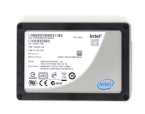
That's the new X25-M G2 I wrote about yesterday, which features a slightly improved controller and 34nm NAND flash. Im hard at work on a full review but I thought I'd share some preliminary data with you all.
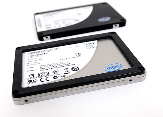
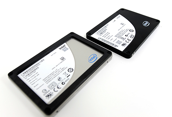
As I mentioned yesterday, the new drive has a silver enclosure. Intel says the new enclosure is cheaper than the old black one:
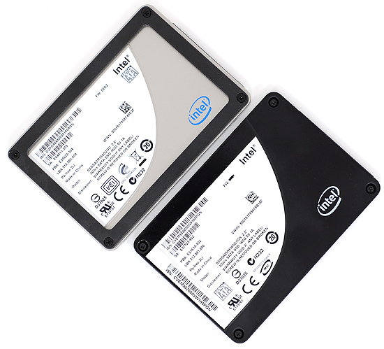
The X25-M G2 (top) vs. the X25-M G1 (bottom)
Our sample also shipped with a plastic spacer so the drive can be used in 9.5mm 2.5" bays as well as 7mm bays by removing the spacer.
![]()


87 Comments
View All Comments
velis - Friday, July 24, 2009 - link
So you don't wonder too much any more:RE: How Come Intel Can't Compete The Sequential Performances Of Its Rivals?
by Anand Lal Shimpi, 1 days ago:
I'm not sure it's a question of why Intel can't, I think it's a conscious architectural decision. It's something I've been chasing down for months but I can't seem to put my finger on it just yet.
This is indeed an implementation decision.
The difference between "ordinary" drives and the Intel drives is in the way they write data to the disk:
"Ordinary" drives can have "high" sequential throughput because they employ only coarse levelling algorithms. That is, they keep erasure counts for entire blocks and write data to the block that currently has the lowest erasure count.
First a bit of glossary for the terms I use:
Block - the smallest unit on a flash chip that can be erased by erase command (typically 256MB).
Sector - The smallest data unit controller's algorithm recognizes. This is probably not equal to 256 or 512 bytes (actually it's a bit more for CRCs and stuff) which is a typical sector size on a flash chip because the reallocation tables would take way too much space then.
Below I only explain the reallocation algorithm - which is in reality also complemented by a wear leveling algorithm (the wear leveling you already know and understand).
Intel's controller (also OCZ Vertex) do this differently: they convert all writes to sequential where they look for the block which has the most "free" sectors. Of course some weal leveling is also applied. So each write is preceded by a lookup of such a block, then this block is erased, the non-free sectors re-written to it along with the new sector.
This method creates massive fragmentation issues and to keep track of it, some quite large lookup tables have to be maintained in the controller.
In order for this method to work as efficiently as possible, it is always good to leave some space on the disk free for the algorithm itself. I know the disk itself doesn't have 80GB capacity, more like 70 available for an OS to use. I wouldn't be surprised if the amount of flash chips on the disk itself was more than 80GB, but I just checked out the PCB pics and this doesn't seem to be the case.
The translation / lookup tables take 1MB per 1GB of storage space if "cluster" size is 4KB, which I strongly suspect it is (default FS cluster size for many file systems). Additionally you need derived "free sector" tables which are also quite large and barely fit into that poor 128Mbit SRAM chip that's there on the PCB if at all. This is only for the most simple implementation os sector reordering algorithm. In order to make things faster, they probably need even larger / more tables.
This free space on the disk simulates the announced TRIM support. Since you always have a certain percentage of the drive "free" for your algorithm to use, you can always assume (and be right) that you will find a block that has at least some sectors free. Since typical disk writing occurs mostly in a few clusters, this then translates into "the same" blocks alternating among themselves.
The reason intel's drives showed performance decrease when in "used" state (BTW: this state is achieved at the same moment when you have written disk's capacity blocks to the disk, but it doesn't mean that the disk is at that time full - it just performed, say 80GB of writes) is because at that particular moment the disk itself has run out of 100% free blocks and it has to start looking for blocks that have as many as possible free sectors. But, naturally, only rarely are those blocks >50% free so writing speed decreases because after block erasure, the controller must write back the sectors that were already full in the block.
So, supporting TRIM will improve the situation for these disks because more sectors will be marked as free. They will still suffer some performance degradation, but not nearly as much as G1 models. Of course this will hugely depend on the amount of disk space that is actually taken (what explorer reports as used capacity). The more free space on the disk, the more sectors "TRIMmed" on the disk itself and the more free sectors to use when writing.
It will also not be necessary to wipe the drive when the TRIM support is installed. It will only take a bit longer for most of the sectors to actually become marked as TRIMmed. So the benefit will be there. But I can't be sure what will happen to the drive's data when the new firmware is flashed on it. If the flashing process or algoritm differences (there shouldn't be any) should wipe the data from the disk, the TRIM benefit will then only come with a wiped drive, won't it?
Also even generation 1 drives should exhibit a lot less "used state syndrome" if they were "resized" to a smaller size. 40GB (half the disk) should be small enough for the degraded performance to never show. Unfortunately I can't test this since I don't have an Intel SSD.
So, finally, to answer the question:
Intel's drives have lesser sequential performance (in theory) than "ordinary" SSD drives because they perform sector reallocation. This algorithm takes it's processing time and the controller chip isn't exactly a 253THz organic computer - if you know what I mean. Additionally, the reallocation tables are quite large and need to be written to the disk along with the data sectors. The ordinary disks have only small reallocation tables and don't suffer so much from having to write them.
has407 - Friday, July 24, 2009 - link
1. Intel spec's 312,581,808 user-addressable sectors = 160GB excluding a "small portion for NAND flash management". Most of that management overhead is below the visibility of the user, and at worst likely to be ~3-5% even if they subtracted all of the overhead from the user-accessible space.2. A "page" is the smallest unit recognized by a NAND unit--that is, the smallest unit of data that can be read or written. Pages are grouped into blocks. A block is the smallest unit that can be erased. A page must be erased--or more accurately in the unprogrammed state--before it can be written/programmed.
a) You don't need to "write back sectors" (pages) unless you are overwriting an existing page; doing so would simply prematurely degrade the flash. The algorithm is: Has this *page* been programmed? No: write it, end; Yes: Does the block contain other valid pages? Yes: Read valid pages, erase block, write back valid pages and new page, end. Obviously you'd prefer to find a unprogrammed page rather than go through the read-write cycle.
b) We don't know the geometry of the Intel flash chips; specifically the page and block size. However, the ONFI 1.0 spec (on which Intel says these are based) states "The number of pages per block shall be a multiple of 32."
3. All reasonable implementations perform remapping as part of wear levelling. Ideally that remapping should be at the page level, as that is the smallest unit of programming (which may be larger than a sector); you also need to keep track of the number of erase cycles for each block.
a) Page mapping requires LOG2(number of pages) bits for the remap table for each page. E.g., for 160GB and page size of 4KB; then: # pages/entries = ~39M; bits/entry = LOG2(39M) = ~25 bits/entry = rounding up to the next byte = 4/bytes/entry * 39M entries = ~160MB
b) Erase cycle counts requires either a counter for each block, a FIFO/LRU that orders blocks based on preference for next write, or more likely a combination of the two (the latter optimized for run-time to answer the question "which page should I write next?").
c) Assuming an erase cycle granularity of 1/2^16 (i.e., a 16-bit counter for each block), a page size of 4KB, a block size of 32 pages (128KB), then for a 160GB drive = 2 bytes/block * ~9.7M blocks = ~20MB. (Again, however, trying to maintain a sorted list of counters is probably not the most efficient way to determine "where should I write next?).
4. Given the above assumptions, the total in-memory wear-leveling overhead for a very reasonable and high performance algorithm for a 160GB drive is ~180MB, less with a bit of optimization. From that we can posit:
a) The page and block sizes are larger than assumed above (less memory needed).
b) The Intel controller has quite a bit of RAM (above the external 32MB DRAM chip).
c) The Intel controller is partitioning operations (reduce the amount of memory required at any time).
d) Something else.
In short, it is far from apparent why differential between Intel's and the competition's serial vs. random IO performance. By all means if you really do know, please explain, but your previous "explanation" appears dubious at best, and ill-informed at worst.
velis - Monday, July 27, 2009 - link
Sorry, had no intention to offend you.However:
The difference between user addressable blocks and actual flash size is quite substantial:
On the PCB you have 160GB of flash (160 * 1024^3 = 171798691840 bytes). Of that, you have 160 billion bytes (~160 * 1000^3) user addressable.
That's almost 11GB difference. Even if my info about disk free space is incorrect, this difference makes up for almost 7% of algorithm useable sectors. Flash chips do come in power of 2 capacities, unlike rotating platter disks.
Your calculations for the tables taking 180MB therefore still leave almost 11GB for the reallocation sectors.
I have also tried to be as plain as possible in describing the algorithm. I delved in no details, but if you insist:
It's impossible to retain information in RAM, be it on controller or on the external RAM module. So no tables there, only cache.
Your calculations actually just "specify" what I told in general terms. For such specification and detailed calculations you would have to actually know the actual algorithm employed.
Your assumption a is incorrect because there's enough space for the tables, so no compressio / optimization is necessary.
Your assumption b probably fails, controllers typically don't have massive amounts of ram. Even if there was massive ram in there, it would still only be used as cache.
I don't see how partitioning operations would reduce disk space requirements, but I believe that partitioning is done. Partition being one sector (smallest storage unit size).
There's probably quite a few "something elses" in there. With only 7% of spare disk space to work with, the algorithm is IMHO a lot more complex than I suggested.
So - why slower seq writes (in a bit more detail):
The controller has to read reallocation tables for the relevant tables. That may mean more than one sector, probably more like 3 or 4, depending how deep the reallocation tables trees are.
Then the sector's physical position is determined and it is written and - if it's time, the modified reallocation tables are written too.
Both reading and writing "excess" information take time. As well as the calculation of the appropriate new address.
I don't know if that's what Intel implemented, but it seems to me a good guess, so don't beat me over it.
has407 - Monday, July 27, 2009 - link
Apologies, that last statement in my previous post was unwarranted. No you didn't offend me, and I didn't mean to beat you up, I was just being a cranky a*hole. Again my apologies.My comments were primarily directed at controller run-time memory overhead, not overhead within the flash device itself. As you said, controllers aren't likely to have that much memory; specifically, sufficient for an in-memory logical-to-physical (LBA-PBA) map for every page of the SSD (never mind for every sector).
Yes, there is going to be some storage overhead; specifically, that needed for garbage collection and long-term wear leveling, where unused pages are coalesced into free blocks (improve write speed), and data in blocks with low erase counts are redistributed (improve longevity).
The importance of the latter is often overlooked, and if not done will lead to premature failure of some blocks, and result in diminishing capacity (which will tend to accelerate). E.g., you load a bunch of data and never (or rarely) modify it; without long-term leveling/redistribution, writes are now distributed across the remaining space, leading to more rapid wear and failure of that remaining space.
I expect they're doing at least garbage collection, and I hope long-term leveling, and may have opted for more predictable performance by reserving bandwidth/time for those operations (write algorithm treats random IO as the general case, which would play to SSD's strengths). OTOH, it may be a lot simpler and we're just seeing the MLC write bandwidth limits and housekeeping is noise (relatively speaking); e.g., ~7MBs for 2-plane x8 device = X 10 channels = ~70MBs.
I won't lay claim to any answers, and AFAICT the simple/obvious explanations aren't. The only thing clear is that there's a lot of activity under the covers that effects both performance and longevity. Intel has done a pretty good job with their documentation; I'd like to see more from the rest of the vendors.
velis - Friday, July 24, 2009 - link
Oops: Block size is 256 KB, not MBrcpratt - Thursday, July 23, 2009 - link
Now on newegg, fyi.StormyParis - Thursday, July 23, 2009 - link
I'm deeply bothered by the disapearance of the tests that showed (only) 25% better level-loading times, and my comments about that.I thought Anand was one of the last intelligent and honest sites around. Good bye guys, it's been nice while it lasted.
Kougar - Thursday, July 23, 2009 - link
Noticed that on the last page the Random Read and Random Write charts need to be switched to align with the actual text above/between them.jimhsu - Thursday, July 23, 2009 - link
Pure conjecture, but read this, specifically page 14:http://www.imation.com/PageFiles/83/SSD-Reliabilit...">http://www.imation.com/PageFiles/83/SSD-Reliabilit...
Possibly Intel is using a longer BCH error correction code to get the 10-15/bit BER rate?
jimhsu - Thursday, July 23, 2009 - link
Also interesting from there was the fact that errors in hard drives usually occur in bursts i.e P(error in bit b|error in bit b-1) is high vs. errors in SSDs which are basically randomly distributed.