AMD Athlon X2 7850 vs. Intel Pentium E5300: Choosing the Best $70 CPU
by Anand Lal Shimpi on April 28, 2009 11:00 AM EST- Posted in
- CPUs
AMD celebrates its 40 year anniversary next month, and the Athlon brand turns ten shortly thereafter. What better way to celebrate than by releasing a rebadged 65nm Phenom processor with two cores disabled at $69? Er, or, I guess they could’ve sent a cake.
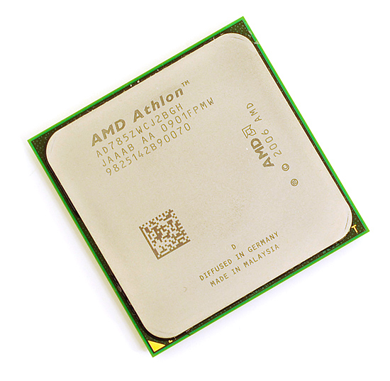
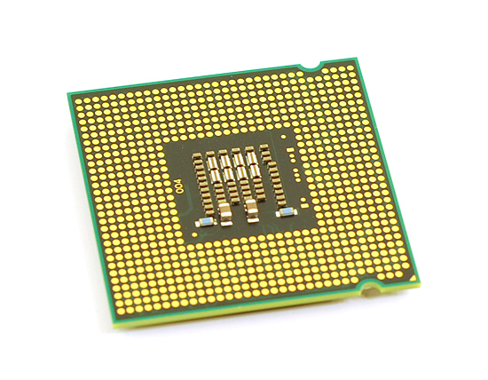
It’s called the Athlon X2 7850 and it actually has very little in common with the old Athlon 64 X2s. As I mentioned, these are rebadged 65nm Phenom processors with two cores disabled. The table below should give you a good comparison between the die size and transistor count of the original Phenom compared to the new Athlon X2:
| Processor | Manufacturing Process | Die Size | Transistor Count |
| AMD Phenom X4 9950 | 65nm | 285 mm2 | 450M |
| AMD Athlon X2 7850 | 65nm | 285 mm2 | 450M |
There’s no surprise that the specs are identical, because the processors are identical. AMD simply disables two of the Phenom’s four cores in production before shipping the parts.
In its heyday the original Phenom never broke 2.6GHz, but with a fully mature 65nm process and only two functional cores AMD is able to clock these parts higher. The first dual-core Phenom derivative was the Athlon X2 7750 and it ran at 2.7GHz. In AMD’s tradition of introducing far too many CPUs, today AMD expands the list with a 2.8GHz Athlon X2 7850.
Once again this is the original Phenom processor; none of the advancements found in the Phenom II are included - it also means that the architecture doesn’t make quite as much sense.
It's a Socket-AM2+ Processor
The original Phenom architecture was designed to be used for quad-core processor designs, hence the use of a large shared L3 cache alongside private L2 caches. With only two cores, many of the benefits of this architecture are lost. Intel discovered that the ideal dual-core architecture featured two levels of cache with a large, fast, L2 shared by both cores. AMD and Intel came to the conclusion that the ideal quad-core architecture had private L2 caches (one per core) with a large, shared L3 cache. The Athlon X2 7850 takes the cache hierarchy of the ideal quad-core design and uses it on a dual-core processor.
To make matters worse, it does so with an incredibly small L3. Intel found that on its Nehalem processor each core needed a minimum of 2MB of L3 cache for optimal performance. With Phenom II AMD settled on 1.5MB L3 per core. The original Phenom gave each core 512KB of L3, or in the case of a dual-core derivative 1MB of L3 cache. Again, not ideal.
But it only costs $69.
And things should be easier for AMD at the $69 price point - there’s no Nehalem to worry about down here, only cache starved Core 2 processors. Priced at $74 we have Intel’s Pentium E5300.
It’s a Difference of Cache
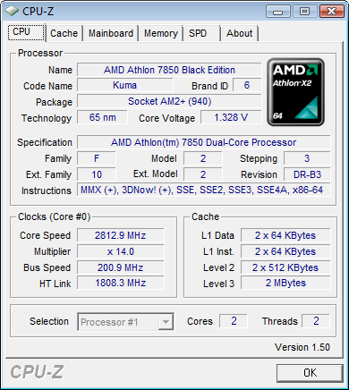
The Athlon X2 7850 is based on the original 65nm Phenom core, but with only two cores enabled. That means we’ve got a 64KB L1 data cache, 64KB L1 instruction cache and a 512KB L2 cache per core. There’s also this catch-all 2MB L3 cache, but it’s unfortunately very high latency by comparison.
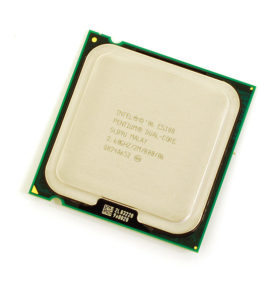
The Pentium E5300
The Pentium E5300 is a trimmed down version of Intel’s 45nm Wolfdale core. Each core has a 32KB L1 data cache and a 32KB L1 instruction cache, smaller than the Athlon X2. The L2 cache is shared between the cores and is 2MB in size. It takes just as long to access data from Intel’s 2MB shared L2 as it does to get data from AMD’s 512KB L2. Intel does not have an L3 cache but it also doesn’t have an on-die memory controller, so final accesses to memory are a lot slower on Intel’s hardware.
It's all LGA-775
AMD has more cache but it’s slower than Intel’s, once you get out to main memory the Athlon X2 can get to data quicker but the E5300 has the benefit of more advanced prefetchers.
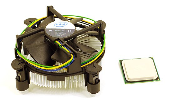
The E5300 is a 45nm chip meaning it can be cooled by Intel's low profile boxed heatsink
Intel’s architecture also has a wider 4-issue front end compared to the Athlon X2. The execution advantage should go to Intel. With a higher IPC, Intel doesn’t need to run at the same clock speeds to outperform AMD. However with an on-die memory controller, the Athlon X2 could pull ahead in applications that don’t fit nicely within the E5300’s L2 cache.
While the Phenom II has been enjoying clear victories over Intel’s equivalently priced processors in the higher end space, it looks like crowning a winner at $70 will take a little more work.


55 Comments
View All Comments
v12v12 - Tuesday, April 28, 2009 - link
What does personal mud slinging have to do with my points? Please debate them, if you can?Doc01 - Tuesday, July 27, 2010 - link
Athlon has surpassed all expectations, Athlon outside competition.<a href="http://www.salesgeneric.net">http://www.sa...
just4U - Tuesday, April 28, 2009 - link
I think overclocks are a non issue with the 5300. Why would anyone buy it over a 5200 which is already a proven performer. Not like the 5300 could actually outdue it... Anyway..I was faced with a decision on a couple of cheap builds. (no overclocking) The 5200 or the 7750. In the end I opted for the 7750 for a few reasons..
I kinda felt that the chips were comparable overall.. but a key deciding factor was the motherboards used. The 780G chipset is just way to tempting at such a low low price for a budget build that it sort of trumps Intel's cpu/mb considerations. Atleast in my opinion... am I wrong?
TA152H - Tuesday, April 28, 2009 - link
Anand, you mention the Pentium has a one cycle faster L1 cache, but my understanding is they are both three cycles. I know the K7 and K8 were three cycles. Did AMD slow down the L1 cache on the Phenom's?A few other things to consider. The L2 cache on the AMD is exclusive, Intel's is inclusive. But, the L1 cache of AMD processors is not really 128K, since they pad instructions for easier decoding, but I guess that's just nitpicking.
I'm really curious about the L1 cache latency though. Can you let us know if the Phenom is now 4 clock cycles? It's an ugly trend we're seeing, with the L1 cache latency still going up, except for the Itanium. Which, as we all know, will replace x86. Hmmmm, I guess Intel missed on that prediction :-P .
Anand Lal Shimpi - Tuesday, April 28, 2009 - link
You know, I didn't even catch that until now. I ran a quick latency test that reported 4 cycles but the original Phenom (and Phenom II) both have a 3 cycle L1. I've got a message in to AMD to see if the benchmark reported incorrectly or if something has changed. I'm guessing it's just a benchmark error but I want to confirm, I've seen stranger things happen :)Intel found that the 4 cycle L1 in Nehalem cost them ~2% in performance, but it was necessary to keep increasing clock speeds. I'd pay ~2% :)
Take care,
Anand
TA152H - Tuesday, April 28, 2009 - link
I was under the impression the reason Intel increased L1 cache latency was so they could use a lower power technology, and save some power.I heard the number was around 3 to 4 percentage loss in performance, but I guess it always depends on workload and who in Intel is saying it.
But, the whole setup seems strange to me now. Typically, when you go to the 3-level cache hierarchy, you see a smaller, faster L1 cache, not a very slow one like the Nehalem has. Especially with such a small, fast L2 cache, and the fact the L1 is inclusive in it, I'm not clear why they didn't cut the L1 cache in half, and lower the latency. You'd cut costs, you'd cut power, and I'm not sure you'd lose any performance with a 32K L1 cache with three cycles, instead of a 64K with four, when you have a 10 cycle L2 cache behind it. A non-exclusive L2 cache that is only four times the size of the L1 cache seems like an aberration to me. I wouldn't be surprised if this changed in some way for the next release, but I have no information on it at all.
But, mathematically, if you could but the L1 cache to three cycles by going to 32K, that would mean you'd get better performance for reads up to the 32K mark by one cycle, and worse by six cycles for anything between 32K and 64K. Typically, you'd expect this to favor the smaller cache, since the likelihood of it falling outside the 32K but within the 64K is probably less than 1/6 the chance of it falling inside the 32K. Really, we should be halving it, since it's instruction and data, but I think it's still true. On top of this, you'd always have lower power, and you'd always have a smaller die, and generate less heat. And you wouldn't have that crazy four to one L2 to L1 ratio.
But, the Nehalem has great performance, so obviously Intel knew what they were doing. Maybe they were able to hide the latency well beyond simple mathematics like I used above, or maybe cutting it to three cycles would have been difficult (very hard to imagine since it's working on the Penryn with 64K, and the clock speeds aren't so different). I wish I knew :-P .
Thanks for your response.
Anand Lal Shimpi - Tuesday, April 28, 2009 - link
This is what I wrote in my original Nehalem Architecture piece:"The L1 cache is the same size as what we have in Penryn, but it’s actually slower (4 cycles vs. 3 cycles). Intel slowed down the L1 cache as it was gating clock speed, especially as the chip grew in size and complexity. Intel estimated a 2 - 3% performance hit due to the higher latency L1 cache in Nehalem."
I believe Ronak Singhal was the source on that, the chief architect behind Nehalem.
I suspect the decision to stick with a 64KB L1 (I + D) instead of shrinking it has to do with basic statistics. There's no way the L1 is going to catch all of anything, but the whole idea behind the cache hierarchy is to catch a high enough percentage of data/instructions to limit the number of trips to lower levels of memory.
It's not impossible to build a 64KB 3-cycle L1, but if Ronak is correct then even a smaller L1 would not negate the need to make it a 4-cycle cache - the L1 was gating clock speed.
I think Intel found the right L1 size for its chips and the right L2 size. The L3 is up in the air at this point. Ronak said he wanted a larger cache, but definitely no less than 2MB per core (8MB for a quad-core).
Take care,
Anand
f4phantom2500 - Tuesday, April 28, 2009 - link
seriously, most people who come to anandtech and look at these things are at least aware of overclocking, if not overclockers themselves. whenever i build desktop rigs for myself i always go for the cheap "low end" chips and overclock them. the e5300 is an excellent example. honestly i'd expect it to completely decimate the 7850 in all ways if they were overclocked, but they should definitely have put it in this review, as there are 2 people who buy these types cheap cpus:1. people who do basic stuff and don't really care anyway
2. people who overclock
and people who overclock would most likely constitute the majority of the readers of a comparison between the two chips, because if you didn't care about performance that much then there aren't too many reasons why you'd bother reading this review.
sprockkets - Tuesday, April 28, 2009 - link
For me, it comes down to whether I want a Zotac mini ITX board based on the 8200 or 9300 chip. While the AMD one is cheaper, they neglected to put in a HDMI and SPDIF ports on it, so, I have to go for the Intel board.Besides, they have a small heatsink fan combo. I assume the AMD one is bigger, but of course, it mounts much easier and better than Intel's setup.
leexgx - Sunday, May 3, 2009 - link
the intel one make so little heat does not need an big heatsink, i going to have to start useing intel CPUs for my basic systems soon as where i get me cpus form only stock 2.7ghz amd X2 CPUs or the heat moster 7750