Intel's 32nm Update: The Follow-on to Core i7 and More
by Anand Lal Shimpi on February 11, 2009 12:00 AM EST- Posted in
- CPUs
The Manufacturing Roadmap
The tick-tock cadence may have come about at the microprocessor level, but its roots have always been in manufacturing. As long as I’ve been running AnandTech, Intel has introduced a new manufacturing process every two years. In fact, since 1989 Intel has kept up this two year cycle.
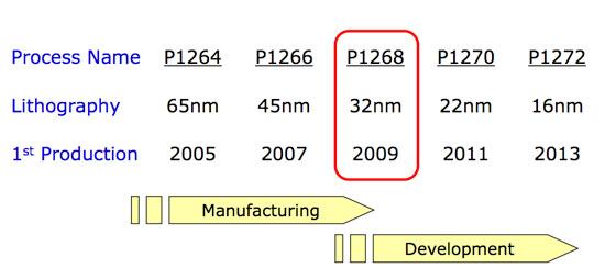
We saw the first 45nm CPUs with the Penryn core back in late 2007. Penryn, released at the very high end, spent most of 2008 making its way mainstream. Now you can buy a 45nm Penryn CPU for less than $100.
The next process technology, which Intel refers to internally as P1268, shrinks transistor feature size down to 32nm. The table above shows you that first production will be in 2009 and, after a brief pause to check your calendars, that means this year. More specifically, Q4 of this year.
I’ll get to the products in a moment, but first let’s talk about the manufacturing process itself.
Here we have our basic CMOS transistor:
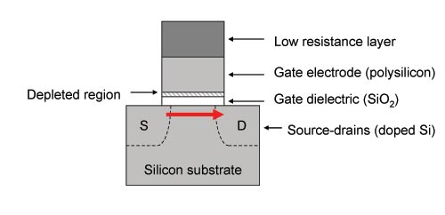
Current flows from source to drain when the transistor is on, and it isn’t supposed to flow when it’s off. Now as you shrink the transistor, all of its parts shrink. At 65nm Intel found that it couldn’t shrink the gate dielectric any more without leaking too much current through the gate itself. Back then the gate dielectric was 1.2nm thick (about the thickness of 5 atoms), but at 45nm Intel’s switched from a SiO2 gate dielectric to a high-k one using Hafnium. That’s where the high-k comes from.
The gate electrode also got replaced at 45nm with a metal to help increase drive current (more current flows when you want it to). That’s where the metal gate comes from.
The combination of the two changes to the basic transistor gave us Intel’s high-k + metal gate transistors at 45nm, and at 32nm we have the second generation of those improvements.
The high-k gate dielectric gets a little thinner (equivalent to a 0.9nm SiO2 gate, but presumably thicker since it’s Hafnium based, down from 1.0nm at 45nm ) and we’ve still got a metal gate.
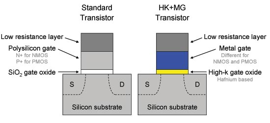
At 32nm the transistors are approximately 70% the size of Intel’s 45nm hk + mg transistors, allowing Intel to pack more in a smaller area.
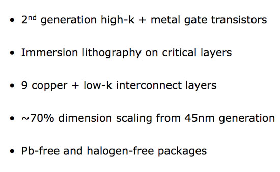
The big change here is that Intel is using immersion lithography on critical metal layers in order to continue to use existing 193nm lithography equipment. The smaller your transistors are, the higher resolution your equipment has to be in order to actually build them. Immersion lithography is used to increase the resolution of existing lithography equipment without requiring new technologies. It is a costlier approach, but one that becomes necessary as you scale below 45nm. Note that AMD to made the switch to immersion lithography at 45nm.
![]()
Intel reported significant gains in transistor performance at 32nm; the graphs below help explain:
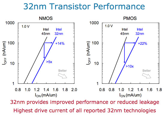
We’re looking at the comparison of leakage current vs. drive current for both 32nm NMOS and PMOS transistors. The new transistors showcase a huge improvement in power efficiency. You can either run them faster or run them at the same speed and significantly reduce leakage current by a magnitude of greater than 5 - 10x compared to Intel’s 45nm transistors. Intel claims that its 32nm transistors boast the highest drive current of all reported 32nm technologies at this point, which admittedly there aren’t many.
The power/performance characteristics of Intel’s 32nm process make it particularly attractive for mobile applications. But more on that later.


64 Comments
View All Comments
tacoburrito - Wednesday, February 11, 2009 - link
I fail to see the purpose of introducing the 6 core/Gulfstream. Most software could barely take advantage of 4 core, let alone 6. It seems like Intel just want to brag they can cram many cores into a single package without evidence that 6 cores will improve performance. It's almost like the mhz wars from the 1990s. Instead of spending time on a 6 core chip, why couldn't they just bring out Sandy Bridge earlier?aeternitas - Friday, February 13, 2009 - link
It cant be that the applications that DO have multicore support arnt professional apps that small and large businesses use to make money now could it?Simple because Intel doesn't cater to your browsing and downloading torrents needs doesn't mean its not a good idea to get the ball rolling.
Oh and hmm, lets see why don't they just go strait to Sandy Bridge that's a good one hmmm maybe its because they DONT HAVE TO. AMD is 18 months behind.
7Enigma - Thursday, February 12, 2009 - link
Check back a couple pages, I think we posted exactly the same thing, as I completely agree with you. :)The only thing I can think of is since the server market pays the bills in a sense they are tailoring the chip for that purpose and just making a consumer level chip that will still be tops but probably not as nice in most instances as a faster quad.
pattycake0147 - Wednesday, February 11, 2009 - link
On the first page the article talks about two Arizona fabs, but the picture indicates that there is one Arizona fab and one New Mexico fab. So which is correct?scruffypup - Wednesday, February 11, 2009 - link
If I remember right (living here in the Phoenix area), there are 3 buildings in Chandler at the site,... 2 of them will be coverted over to the 32nm process, the 3rd building is no longer going to be used apparently,.... or will use the 3rd for something else,...http://www.intel.com/community/arizona/index.htm">http://www.intel.com/community/arizona/index.htm
http://www.azcentral.com/arizonarepublic/business/...">http://www.azcentral.com/arizonarepubli.../2009/02...
"Specifically, Intel is upgrading two of its three manufacturing plants, called "fabs," at its Ocotillo campus in Chandler to make 32-nanometer-size chips."
INDVote - Thursday, February 12, 2009 - link
No, only one fab in AZ is being converted, Intel's newest Fab 32. They are not closing any one or both other buildings. They appear to be "merging" two of them.F11X is in New Mexico, and will be converted over. There are no plant closings in NM.
D1D and D1C are both at the same location in Oregon and are being converted.
pattycake0147 - Wednesday, February 11, 2009 - link
However, the three buildings combined are called Fab 32. Fab 11X as chopshiy pointed out is in New Mexico. The article isn't referring to individual buildings, but sets of buildings.Thanks chopshiy, I didn't see your post earlier.
vlado08 - Wednesday, February 11, 2009 - link
I am wondering about the integrated graphics in Clarkdale/Arrandale will it be DirectX 11 compliant? Is it going to be better than GMA X4500? What about h264 acceleration, 8 channel LPCM support and working 24p?chophshiy - Wednesday, February 11, 2009 - link
11X is in New Mexico as the caption on the pic says. Specifically Rio Rancho, NM, near Albuquerque. It's OK, you'd be surprised how many times I've spoken with someone in the US on the phone that told me I was calling the wrong number, since they don't support locations outside the US. Go American education!philosofool - Wednesday, February 11, 2009 - link
Does anyone know what the lifespan of LGA 1156 will be? Is intel expected to change sockets again when we reach Sandy Bridge? Is there any chance that I will have be able to get one mother board to last me several years?