The RV770 Story: Documenting ATI's Road to Success
by Anand Lal Shimpi on December 2, 2008 12:00 AM EST- Posted in
- GPUs
Re-evaluating Strategy, Creating the RV770 in 2005
Remembering what lead to success rather than the success itself is generally more important, and around 2005 ATI had another R300 moment. What made R300 successful was ATI re-evaluating the way it made GPUs and deciding on something that made sense. At the time, it made sense for ATI to work towards building the biggest chip possible, win at the high end and translate that into better, more competitive products at all other price points. It is worth mentioning that part of R300’s continued success was due to the fact that NVIDIA slipped up royally with the GeForce FX, it was the perfect storm and ATI capitalized. ATI built the biggest chip and NVIDIA had no real answer for some time to come.
Just as Intel bumped into the power wall when it tried to ramp Pentium 4 clock speeds to ridiculous levels, ATI was noticing that GPUs were getting a little too big for comfort. Design cycles were getting longer, die size was growing and financially there were some things that didn’t quite make sense when it came to making these large GPUs.
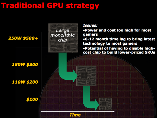
ATI asserted that a very large GPU, without the use of repair structures or harvesting (two techniques I’ll describe in a bit) may only have a 30% yield. That means for every 100 GPUs produced on a single wafer, only 30% of them would be fully functional and could be sold as advertised. Manufacturing these complex circuits is particularly expensive, those fab plants easily cost a couple of billion dollars to build and thus having most of your wafer go to waste isn’t really a good way of running a business.
Thankfully there are ways to improve that crappy 30% yield to a value north of 90%. The first is a technique generally known as repairability. The idea behind repairability is simple: build redundancy into your design. If you have a unit with 10 shader processors, actually build 11 but use one as a spare should there be a defect in any of the remaining processors. The same technique is often used for on-die memory, include additional cells so that a defect in one part of a cache won’t render the entire chip unusable. There are tradeoffs here however, if you build in too much repairability then you run the risk of having a die that’s large but offers no additional performance benefit. If you don’t build in enough repairability then your yield suffers.
Harvesting is another technique that all of you are quite familiar with, although its street name is feature binning. The idea here is that you assume that only a small percentage of the die on a wafer will be completely functional, but instead of throwing away the ones that aren’t fully functional, you disable features and sell them as a lower end part. For example, if your target architecture has 10 shader processors but only 30% of your production will have 10 working shader processors but 50% of the production will have 8 working units you’d sell a model with 10 SPs and a model with 8 SPs, the latter being at a reduced cost. This way instead of throwing away 70% of the wafer, you only throw away 20% - and if possible you could make a third SKU with fewer number of functional SPs and use close to 100% of the wafer.
Yields do improve over time, and what eventually happens if you build a product relying on harvesting is you hurt yourself financially. In the example above where you have two configurations of the same die, yields will eventually improve to the point where your 8 SP die could just as easily have 10 functional SPs but you have to sell them as reduced functionality parts because you’ve built up market demand for them. In a sense, you’re selling something worth $1 for $0.80. You could always create a new version of the chip with a smaller die, but that takes additional engineering resources, time and money.
The most recent public example of die harvesting was actually with NVIDIA’s GT200. The GeForce GTX 260 was simply a harvested version of the GTX 280 with 192 SPs vs. 240. As yields improved, NVIDIA introduced the GeForce GTX 260 Core 216 with 216 SPs. Note that NVIDIA didn’t use any repairability for the shader processors on GT200 there are no more than 240 functional SPs on a GT200 die, but that’s because NVIDIA would rely on harvesting anyway - if any of the 240 SPs didn’t work the chip would be branded as a GTX 260 or Core 216.
This is in stark contrast to RV770 where both versions of the GPU were functionally identical, the only differences were clock speeds and power requirements. But from a die standpoint, ATI didn’t have to sell any reduced versions of the chip to keep yields high.
Note that whether or not a company has to rely on harvesting doesn’t really impact the end user. In this case, the GeForce GTX 260 Core 216 actually benefitted the end user as it manages to deliver the same sort of value that AMD does with the Radeon HD 4870. It isn’t ideal for NVIDIA financially and if a company has to rely on harvesting for too long it will eventually take its toll, but I suspect that in the GT200 case NVIDIA will bail itself out with a 55nm revision of GT200 before things get too bad.
ATI didn’t want to build a GPU that would rely on excessive repair and harvesting to keep yields high. And then came the killer argument: building such a GPU was no longer in the best interests of its customers.
Sidenote: Building a GPU
Before we get too far down the rabbit hole it’s worth adding some perspective. ATI’s RV770 design took three years of work, that means ATI started in 2005. It takes about a year for manufacturability from tapeout to final product ship, another 1 - 1.5 years for design and another year for architecture.
The team that I met with in Santa Clara was talking about designs that would be out in 2012, we’re talking 4 TFLOPS of performance here, 4x the speed of RV770.
Decisions being made today are going to impact those products and in a sense it’s a big guessing game, ATI has no idea what NVIDIA will have in 2012 and NVIDIA has no idea what ATI will have. Each company simply tries to do the best it can for the customers and hopes they’ve got the right mix of performance, price and power.
To give you an idea of the intensity of some of these debates, Carrell debated, every evening, for three hours, for three weeks, the amount of repairability that would go into the RV770. Building redundant structures in the RV770 was an even bigger deal than before because ATI was going to be working within serious die constraints, simply making the chip bigger wasn’t an option. Repair structures in the RV770 wouldn’t add any performance but would increase the die size, on an already large chip that’s fine, but on a chip that’s supposed to target the sweet spot and can’t grow without limit it’s a big deal.


116 Comments
View All Comments
nezuko - Thursday, December 4, 2008 - link
I think those phrase is describe what Graphic-field is. Another year win, and another year lose. But from those situations, only hardworking and tough guy would be able to turn all upside down. And ATi team do make it. Now I relieved I make a decision to buy 4670, though not performance, it still does big bang for the buck. And with those Catalyst 8.12, I would be more grateful that I bought this video card. Has been downloaded it and now testing it.Would Anand make another article about those GP-GPU programming language to make a data parralel computing possible.
Well, I considering to build my Leo Platform in the H2 of 2009 when the AM3 Deneb is out, Sata 3, and RD890.
JimiP - Thursday, December 4, 2008 - link
Like many before me have said, this has to be one of the best articles I've ever read here at AT. It really puts things into perspective. We (the consumer) are always criticizing or praising everything that comes out and don't take into account the amount of hard work and time put into the release. I'm 4850 owner, and I couldn't be happier with the performance I've received. I would like to personally thank ATI/AMD and the entire team that put RV770 into play. Absolutely brilliant.I would also like to thank Anand for sharing this awesome experience with us.
zshift - Thursday, December 4, 2008 - link
I have to say this was a great article. Great idea to write about the story behind these guys and the rv770. musta been a helluva relief when they realized how great the gpus were in the market, especially after taking such huge risks. For these guys to pull through the way they did, with the whole gddr5 issue and the die-shrink/physical limitations is amazing. I thought I was stressed in college. I can't imagine what its like to design something like this for 3 years not being even sure it'll work in the end. That's one hell of a resolve, makes me like ATI a bit more than I already do.Keep writing great articles here, this is my favorite site to read reviews on, and this is another reason why.
go anand! :p
strikeback03 - Thursday, December 4, 2008 - link
I agree with everyone else that the article is very well written. I am not sure if these would even be the right guys to ask, but did you bring up any of the driver issues your other recent articles have mentioned with them? As you have mentioned before, it is probably not the best business plan to assume nVidia will screw up again, and they should probably get their crossfire support in order for the good feelings about this strategy to continue.Dyno1979 - Thursday, December 4, 2008 - link
Definitely one of the best articles I've read lately. And I didn't even notice that typo, probably because I was reading the article instead of looking at it.5 stars
CarrellK - Thursday, December 4, 2008 - link
The "sweet spot" strategy would have amounted to *nothing* without the efforts of many very talented engineers (and a little luck as Anand has noted). They made the 770 happen and deserve the lion's share of the credit.I didn't think Anand would use this for anything other than background here-and-there in future articles. I fully expected him to politely cut me off at some point and say "about those future architectures..." which would have lead to Eric, Mike, and Mark telling a different interesting story. Thanks to Anand et al for telling this part of the 770 story. Responding to a comment or two in the posts:
* Sorry to quench the speculation - the AMD purchase had no effect on the 770's execution. Dirk Meyer and the other AMD executives supported Rick, a guy that they really didn't know, during some pretty tough times at AMD. They did their jobs so that we could do ours.
* The price range for 770-based cards was determined back in 2005 - it was an essential factor limiting the GPU cost, one of the big gambles. We had no clue what nV's 2008 pricing would be, but we did know what the gamers wanted. At launch we were tempted oh so briefly to launch at a higher price given the competitor's product offerings. It took some will-power for the starving man (us) to pass up a banquet (profits). We had a sneaking suspicion there was a lot of unhappiness about the direction prices had gone, and didn't want to be a party to that for the sake of a few weeks better revenue. Greed never pays. Remembering your customers does.
P.S. We don't keep any dart-board pictures of Anand around the office. However I *do* recall seeing his picture somewhere and thinking at the time that it *would* make a good dart target. Just a thought... :-)
lyeoh - Sunday, December 7, 2008 - link
You guys got the sweet spot right as far as I'm concerned (I'm not sure if it's true for others - does it show up in the units sold?)Before the ATI 3800 (RV670), and Nvidia 8800GT, it seemed like after shelling out a few hundred US dollars, you'd only get low/medium quality at current games. And cheaper cards were pathetic to unusable for new games.
So I stuck to playing old games with on my old video card (Ti4200) - which was decent in its time.
After the beginning of the new "sweet spot" era, this year I bought a 9800GT (and a new PC). While the 9800GT is not as good as AMD/ATI's offerings in hardware performance terms, I was concerned about ATI's drivers/software. A colleague tried an ATI card on his office PC, but in the end he had to switch to Nvidia to get his multiscreen set up on Linux working the way he wanted, and I had seen a fair number of complaints from others. So far Nvidia's drivers have been OK for me whether in Windows or Linux.
On the other hand I've seen too many Nvidia cards failing in hardware terms (bad caps, bad whatever). So pick your poison ;).
But if the cards aren't totally crap, it often takes less time to just replace a faulty card, than to keep tinkering with drivers and software configs (sometimes to no avail).
Anyway, many thanks for helping to make stuff affordable, even though I picked Nvidia again ;).
In the end I'm still back to mostly playing old games though...
MrSpadge - Saturday, December 6, 2008 - link
Thanks Andantech, ATI & AMD for this amazing article!And I'd like to add a point which has not been raised yet, at least in this discussion: the "small and fast enough" strategy only works because GPUs hit the realm where they're power limited!
The point is, whenever you go multi-GPU you loose performance due to inefficiencies and communication delays and there are also some transistors lost to redundant logic. If you had the choice between one 100 Mio transistor chip or 2 50 Mio ones, then the 100 Mio one would certainly be faster; assuming both could run at the same clock speed, which previously was determined by chip design (basically identical in the example) and process (identical).
But GT200 is too big, it can not fully fledge its clock speed wings because its power limited. Imagine GT200 at 1.5 - 1.8 GHz shader clock - it would be much more in line with performance expectations. RV770 on the other hand can be pushed quite a bit and on the 4870 it chews up lots of power for such a small chip - but that's OK because this power envelope has been accepted and the performance is there to justify it. And the 2 GPU versions are succesful because the power envelope on such "freak"-cards is larger.
And another frequently overlooked aspect: not all of GT200s transistors contribute to game performance. The 30 shaders which are 64 bit capable must be large and don't help games at all (and probably won't for quite some time). This is a very forward looking feature for games and a feature of immediate benefit for GP-GPU.
MrS
Frallan - Friday, December 5, 2008 - link
Thank you m8!Not only for delivering good products but also for delivering good information and entertainment.
Please convey to the other "Fellows" the heartfelt thanks of this community.
JimmiG - Thursday, December 4, 2008 - link
Congratulations to Anandtech for one of the most interesting articles this year. Congratulations to ATI/AMD for putting out their best and most exciting product since R300/9700 Pro.The industry really needed something like RV770. When the 9700 Pro came out in 2002, it was at the cutting edge of technology and performance, far ahead of the previous champion, the Ti4600, yet it launched at only $399. Nvidia launched the 8800 Ultra and GTX280 at $800 and $600 respectively, even though neither GPU introduced any significant new features, only moderately higher framerates.
I currently have a 4850 512MB which I bought in July and I love it... It runs all my favorite games at great framerates and with fantastic image quality at 1680x1050. Still, I wouldn't considering myself an "ATI fan". When it's time for me to upgrade again, I will buy the best card in the $200 range and won't care whether the sticker on the GPU fan is green or red.