NVIDIA GeForce GTX 260 Core 216: Competition for the 4870
by Anand Lal Shimpi & Derek Wilson on September 16, 2008 12:00 AM EST- Posted in
- GPUs
Nearly a year ago I wrote about something I called "sensible naming" with respect to GPUs. It was at the time of the Radeon HD 3800 series launch where AMD unveiled a much cleaner, simpler way of naming its cards. Gone were the suffixes (for the most part) and instead what we were left with was this:
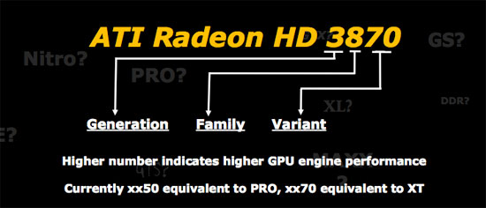
A family name, Radeon HD, followed by a four digit number. With the exception of the X2s, AMD has stuck to its naming system without fault. In fact, AMD has done such a good job with keeping the names clean that things are the way they should be: the internal codenames are more difficult to remember than the actual names of the cards (e.g. RV770 vs. Radeon HD 4870).
NVIDIA however, just hasn't gotten the hint. The GT200 launch gave us two simply named cards: the GeForce GTX 280 and GTX 260, but it didn't take long for NVIDIA to confuse the marketplace with the launch of the GeForce 9800 GTX+. I hoped that the naming silliness was limited to the older GeForce 9 GPUs, but today it extended into the GTX lineup.
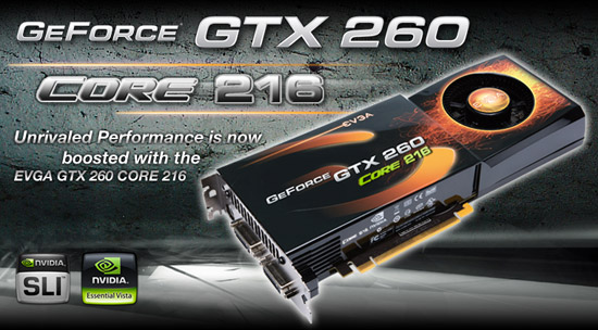
It's called the GeForce GTX 260 Core 216.
Holy nomenclature Batman
The GeForce GTX 260 Core 216's name is actually quite descriptive, albeit absurdly long. The GeForce GTX 260 part we already know from the GT200 launch, the Core 216 suffix just indicates that the GPU has 216 "cores" (also playing on Intel's new Core i7 naming for Nehalem, due out later this year). Why NVIDIA didn't just call it a GeForce GTX 265 or 270 is beyond me. To make matters worse, we'll see companies adding their own suffixes to the already extended name. For example, EVGA sent us their Core 216 called the EVGA GeForce GTX 260 Core 216 Superclocked Edition. Perhaps it's some conspiracy to increase the salary of writers who get paid by the word.
| GTX 280 | GTX 260 Core 216 | GTX 260 | 9800 GTX+ | 9800 GT | |
| Stream Processors | 240 | 216 | 192 | 128 | 112 |
| Texture Address / Filtering | 80 / 80 | 72/72 | 64 / 64 | 64 / 64 | 56 / 56 |
| ROPs | 32 | 28 | 28 | 16 | 16 |
| Core Clock | 602MHz | 576MHz | 576MHz | 738MHz | 600MHz |
| Shader Clock | 1296MHz | 1242MHz | 1242MHz | 1836MHz | 1500MHz |
| Memory Clock | 1107MHz | 999MHz | 999MHz | 1100MHz | 900MHz |
| Memory Bus Width | 512-bit | 448-bit | 448-bit | 256-bit | 256-bit |
| Frame Buffer | 1GB | 896MB | 896MB | 512MB | 512MB |
| Transistor Count | 1.4B | 1.4B | 1.4B | 754M | 754M |
| Manufacturing Process | TSMC 65nm | TSMC 65nm | TSMC 65nm | TSMC 55nm | TSMC 55nm |
| Price Point | $420 - $500 | $279 | $250 - $300 | $200 | $130 - $170 |
If you remember the diagram below from our GT200 review you'll see that a GeForce GTX 280 has ten clusters of 24 stream processors (the little blue blocks), for a total of 240 SPs or "cores". The GeForce GTX 260 has eight of those clusters (called Texture/Processor Clusters or TPCs), bringing its total up to 192 SPs. The Core 216, as you can guess, has nine clusters or 216 SPs. NVIDIA just enabled another TPC on the Core 216 (or alternatively, disabled a TPC on a GTX 280).
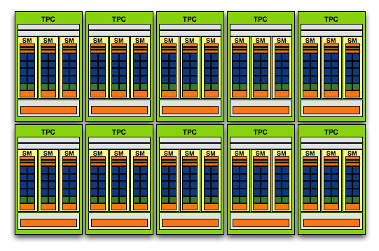
The GeForce GTX 280, 10 TPCs, 240 SPs
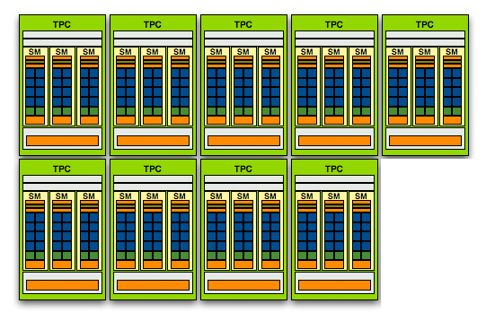
The GeForce GTX 260 Core 216, 9 TPCs, 216 SPs
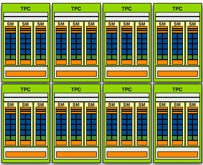
The GeForce GTX 260, 8 TPCs, 192 SPs
The extra TPC also gives the Core 216 another 8 texture address and filtering units, but the rest of the chip's makeup remains the same, even down to the clock speeds. The Core 216 runs its core, shader and memory clocks at the same frequencies as the vanilla GTX 260.
Priced at $279, the Core 216 is a direct competitor to AMD's Radeon HD 4870 - selling at a similar price. The GTX 260 will continue to exist although selling at a cheaper price point and naturally with more processing power, the GTX 280 remains unaffected.


65 Comments
View All Comments
helldrell666 - Tuesday, September 16, 2008 - link
this is a overclocked new 260gtx cuz the stock one has the same clock and shader frequency of the original 260gtx.you should have included a 4870 top or a xoc 4870 in this test.
strikeback03 - Wednesday, September 17, 2008 - link
If you had actually read the article, you would see in multiple places that they ran it at both stock clocks and overclocked (as received) and showed both results.After all the complaining the AMD fanbois did when they showed a 9600GSO in the 4670 article, why would they bring in a new AMD overclocked card and hear the same thing from the NVIDIA fanbois?
toyota - Tuesday, September 16, 2008 - link
what are you talking about? those are the same clocks as the standard GTX260.Staples - Tuesday, September 16, 2008 - link
The ridiculous amount of power draw for an idle card has been going on too long. I have a 4850 and my system consumes 30w more than it did beofre with a 7950GT. Most people do not pay attention to this number but I sure do. I am glad to see that NVIDIA has done more than just bumped up the chips inside this, there is significantly less power draw when it is idle.And here is hoping that ATI can actually come out with some better drivers this month. The 8.8 cause all kinds of trouble with a 780G chipset (in Vista 32) and a 4850 (in XP). Amazing but I have to run 8.7 on both computers because the 8.8 drivers are really problematic.
Vidmo - Wednesday, September 17, 2008 - link
Power Savings??? Where? 160-200 watts for sitting there? Give me a break. These GPUs are a massive waste of power. ATI/nVidia should be ashamed of themselves.MrSpadge - Wednesday, September 17, 2008 - link
Take a calm look at the power consumptions of actual cards, e.g. here:http://www.xbitlabs.com/articles/video/display/zot...">http://www.xbitlabs.com/articles/video/display/zot...
You'll see that the 4870 draws 65 W at idle (seems power play doesn't work there either). Assuming 80% power supply efficiency that means a draw of 81 W at the wall. Therefore ATs system draws 122.5 W without the GPU and the NVs consume about 36 W from the wall and 29 W for the cards themselves. That's way better than previous generation NV cards, which consumed 40 - 60 W at idle. That's what the previous poster meant by "power savings".
(seems like power mixer is not working for XBits NV cards, whereas for ATs it works)
MrS
bespoke - Tuesday, September 16, 2008 - link
I know you were reviewing the chip and not really the EVGA product, but looking at the product images on newegg, I see all the GTX 260s look exactly the same, so the fan noise of this card should be fairly representative for other GTX 260 Core 216s. (Wow, that name is a mouthful.)piroroadkill - Tuesday, September 16, 2008 - link
Why didn't they just call it the Geforce GTX 270cabul - Thursday, May 21, 2009 - link
I read somewhere else recently that it is because the 260 and the 260 Core 216 can still be SLIed together. If they called it anything other than a 260, they felt that consumers would be confused.It makes perfect sense to me now.
gaiden2k5 - Tuesday, September 16, 2008 - link
or GTX 265 since it's a variant of the 260 card