Intel's Larrabee Architecture Disclosure: A Calculated First Move
by Anand Lal Shimpi & Derek Wilson on August 4, 2008 12:00 AM EST- Posted in
- GPUs
Drilling Deeper and Making the AMD/NVIDIA Comparison
Don't be fooled by the initial diagram, this simple x86 core gets far more complex. In the image below, the block to the left is the Larrabee core we mentioned earlier, to the right we've blown up the vector unit and its associated parts:
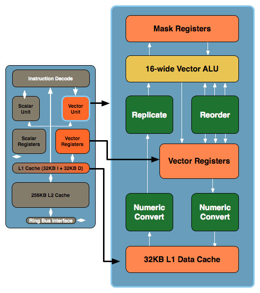
The vector unit is key and within that unit you've got a ton of registers and a very wide vector ALU, which leads us to the fundamental building block of Larrabee. NVIDIA's GT200 is built out of Streaming Processors, AMD's RV770 out of Stream Processing Units and Larrabee's performance comes from these 16-wide vector ALUs:
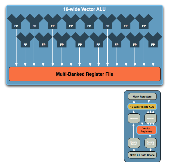
The vector ALU can behave as a 16-wide single precision ALU or an 8-wide double precision, although that doesn't necessarily translate into equivalent throughput (which Intel would not at this point clarify). Compared to ATI and NVIDIA, here's how Larrabee looks at a basic execution unit level:
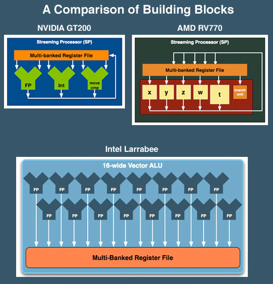
NVIDIA's SPs work on a single operation, AMD's can work on five, and Larrabee's vector unit can work on sixteen. NVIDIA has a couple hundred of these SPs in its high end GPUs, AMD has 160 and Intel is expected to have anywhere from 16 - 32 of these cores in Larrabee. If NVIDIA is on the tons-of-simple-hardware end of the spectrum, Intel is on the exact opposite end of the scale.
We've already shown that AMD's architecture requires a lot of help from the compiler to properly schedule and maximize the utilization of its execution resources within one of its 5-wide SPs, with Larrabee the importance of the compiler is tremendous. Luckily for Larrabee, some of the best (if not the best) compilers are made by Intel. If anyone could get away with this sort of an architecture, it's Intel.
At the same time, while we don't have a full understanding of the details yet, we get the idea that Larrabee's vector unit is sort of a chameleon. From the information we have, these vector units could exectue atomic 16-wide ops for a single thread of a running program and can handle register swizzling across all 16 exectution units. This implies something very AMD like and wide. But it also looks like each of the 16 vector execution units, using the mask registers can branch independently (looking very much more like NVIDIA's solution).
We've already seen how AMD and NVIDIA architectural differences show distinct advantages and disadvantages against eachother in different games. If Intel is able to adapt the way the vector unit is used to suit specific situations, they could have something huge on their hands. Again, we don't have enough detail to tell what's going to happen, but things do look very interesting.


101 Comments
View All Comments
skochnet - Monday, August 4, 2008 - link
I have been a daily reader of Anandtech and computer tech enthusiast for the past 6 years. I found this article so interesting and well written that I felt compelled to signup for an account today to post my appreciation for it. The depth of this article was fascinating. This could be a leap ahead technology which would change and potentially restructure the industry as it stands now if successful. …or not make the grade and the industry players all continue the tug-of-war. I especially enjoy your speculation. Your group is no doubt privy to a unique vantage point that makes these thoughts even more valuable and interesting. Thank you.DerekWilson - Monday, August 4, 2008 - link
We really appreciate the kind words.I'm glad you enjoyed the article, and this is definitely and exciting development that I think -- whether it succeeds or fails -- we will all have our eyes on.
iocedmyself - Monday, August 4, 2008 - link
Actually crysis is the point, or a good example anyway since intel has been touting that larrabee will be something like up to 2.5 - 5 times faster than traditional present day gpu solutions. I didn't think they had been working on this for 4 years, and while it may have seemed like a good idea back then at a time when they hadn't launched a worth while product in 4 or 5 years: they just aren't that innovative.HP and intel teamed up in 94 to develop the original IA-64, spent billions in developement launching it 3 years late and making platform sales in the triple digits...total.
During that time they also started developing the Timna in 97, what was supposed to be for the low-power sub-$600 desktop system bracket and their "first" cpu with an IMC. To achieve this they designed the IMC for use with Rambus memory...they pushed launch back several times to nearly 2 years after projected, during which they redesigned the IMC for use with SDRAM, though it ended up having some pesky fatal design flaw and they scrapped it just before the launch of...
Pentium 4! mmm...netburst, tastes like cowpie. Intel originally quoted netburst as being able to scale to 10Ghz, but they were close there weren't they? 3.8ghz is close...isn't it? It's almost half-way...besides, it doubled as a hotplate!
It has taken them 5 years to reach the point of being able to essentially copy AMD's IMC design, to luanch on a chip which they licsence the x86-64 code from...AMD. Intel may do great work when it comes to designing new motherboard and networking standards (sata, Pci-e, and ehternet) but a high performance 32bit chip launched months before the consumer 64bit OS isn't an achievment in my view, so much as a reminder of the success they enjoyed in the P4 days.
From a performance standpoint, it just doesn't seem realistic. The HD4870xt can surpass 1 teraflop of computations on a single 55nm die, where as Intel's $1000+ highest performing quad-core chips clock in at 38-51 gigaflops or 9.5-12.75 gigaflop per core.
Their 80 core Terascale which used a 65nm fab if i'm not mistaken hit 1 teraflop clocked at 3.2ghz (12.5g Gflop/core) and 1.8 teraflop when clocked up to 5.1ghz (22.5 Gflop/core)
ltcommanderdata - Monday, August 4, 2008 - link
Perhaps it's not so, but it seems to me that Larrabee is quite similar to the SPEs in Cell. Simplified cores based on a common ISA (x86/PPC) optimized for floating point/vector ops. It might be interesting to compare the Cell's and Larrabee's architecture and eventually performance when the products are released. I believe Toshiba is already incorporating the Cell as the Spurs Engine accelerator in notebooks so I can see it running into Larrabee. Might be a return on the x86/PPC debates.Lux88 - Monday, August 4, 2008 - link
I'm glad Intel strongly believes they can provide a solution. Novel approaches are always welcome :)!But there are couple of things that keep me from becoming overly optimistic:
1. Itanium also relied (relies) on very smart compilers to produce the optimal machine code. Didn't quite happen.
2. Dynamic compilers, i.e translationg DirectX to Larrabee on the fly, can't be very smart because this translation has to run in "real time".
3. Intel seems to be heavily touting raytracing. Again, I'm glad they are doing this. But it seems to confirm that they know they can't have a sellar win by just rendering "same old DirectX" through additional layers.
In addition to hardware, they have to juggle with drivers, compilers and libraries. Also came up with software renderer. Also support developers to code great apps on Larrabee (I bet Carmack can't wait to try out his octree-renderer). Quite a number of moving targets to nail down...
DerekWilson - Monday, August 4, 2008 - link
1) Itanium does do certain things very very well -- it's just not the future of the desktop.2) note that we did not use the word emulation or translation at any point -- Intel is NOT doing this with DirectX. It's just like any other API: the DirectX functions that must be implemented in a driver will be implemented in code written for Larrabee as opposed to code written for GT200 or RV770 ... Imagine some other API or even just a DLL with some functions in it -- it's all the same no matter what hardware it's written for. In some cases we'll see the actual implementation just set registers and issue a single command to the hardware to get something done. In Larrabee's case, functions to perform any complex operation will have to be called, but they are essentially doing the same thing.
When I first go started on OpenGL, it was running in software. Hardware companies came along and implemented OpenGL functions in a way that used their hardware. These APIs are hardware independent (essentially).
3) the raytracing talk is, to a degree, posturing. raytracing scales well with traditional CPUs. rasterizers fit well on wide vector hardware. Larrabee happens to be both ... so ... I think they are interested in the long term. honestly, when hybrid renderers come along that combine raytraceing for specific effects inside a rasterizer we'll see some really cool things. I think this is where Intel is going.
NVIDIA even showed off some hybrid tech that could run on their hardware.
...
...
Intel does have a lot of hurdles to get past, and that is definitely worth pointing out.
mars777 - Monday, August 4, 2008 - link
Just one curiosity:A predicted 64 core Larabee would contain 64x32KB of L1 cache and 64x256KB of L2 cache.
- 2048 KB of L1 + 16328 KB L2 -
Given a chess field configuration on silicon this lead to an abnormal die size with too much parallel leaking lines where cache coherency will be impossible or given a 4/8 block configuration which leads slower L2 cache (but this means these are not just cores sticked on silicon but rather a custom core which defeats the purpose of the project and makes this a pretty $$ solution).
IMHO Larabee will probably work out but will be nothing to cheer about, probably a pushed up product that will eventually die out slowly (itanium...).
DerekWilson - Monday, August 4, 2008 - link
itanium has what? 24mb of on die cache? Large cache is not unreasonable for something like this -- but you are forgetting register space and the fact that the L1 has both 32k data and 32k instruction (so 64 cores would be 4MB of L1)The L2 cache is segmented so that each core can only directly access 256kb. The arrangement can be quite flexible because of this. Cache coherency is maintained through the ring bus. if one core needs data being used by another core, in the L2, it goes through the ring. at least that's my understanding.
I apologize if we didn't do a good enough job in the article, but this isn't just a solution where Intel wants to drop stock cores on a die -- everything is custom from the scalar and vector processor upto the internal memory bus and added fixed function logic.
the project has been in development for 4 years and is not meant to be cheap -- intel is putting a lot into it.
by the way -- i still think 32 cores is the sweet spot for launch based on the data Intel provided -- I don't think they'll target a larger size off the bat.
Griswold - Monday, August 4, 2008 - link
One of the few comments here that actually make sense.FujiT - Monday, August 4, 2008 - link
Some if you just don't get it.It's not about whether or not it can play crysis with 100 FPS and it's not as much about whether it can compete with AMD/nVidia (although that's important too).
I see this chip as a beginning of a new revolution in computing. It reminds me a lot of a cell processor (although i don't know that much about architecture) where a smarter CPU will tell the dumber CPUs what to do. The ability to have a many core CPU with a mixture of really smart and dumber, but FP optimized cores will really make stuff like rendering a lot faster on a CPU, and would take programs such as F@H to the next level. The added perk is the fact that it's all x86 as anand pointed out.