AMD's SB750: Enabling Higher Phenom Overclocks?
by Gary Key on July 23, 2008 12:00 AM EST- Posted in
- CPUs
The web has been alive with rumors of an upcoming update to AMD's 7-series chipsets that will somehow unlock the true overclocking potential of its Phenom processors. The rumor goes something like this: an updated South Bridge (SB750) will improve communication with Phenom, removing a previous bottleneck and improving the maximum overclock possible. We can't begin to explain the many issues with the various rumors, but we have to allow that somewhere buried deep in these rumors there is a morsel of truth.
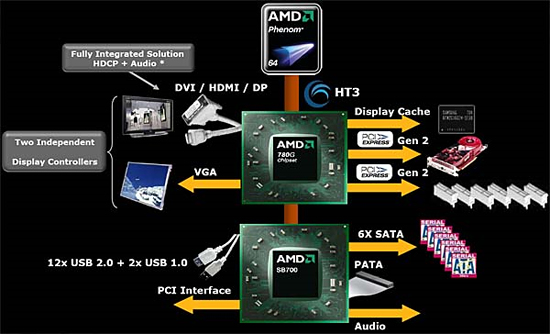
The AMD 780G chipset, the South Bridge is the chip, er, at the south end of the image. USB, SATA and Audio all stem off of this chip.
The South Bridge of a chipset is typically responsible for I/O operations. The non-critical PCIe lanes come off of this chip, as do the SATA and USB ports. Audio codecs, networking interfaces and virtually all other components are also run off the South Bridge. The North Bridge on the other hand talks directly to the CPU and connects it to much higher speed elements of the system; things like graphics cards and main memory all stem from the typical North Bridge design. The point of this explanation being that if anything were going to improve overclocking performance, we would assume it would be the North Bridge, not the SB. However, AMD has taken a different approach from traditional chipset engineering as we will soon see.
We've been waiting for a motherboard with AMD's SB750 South Bridge ever since we started hearing these rumors, and we finally received one:
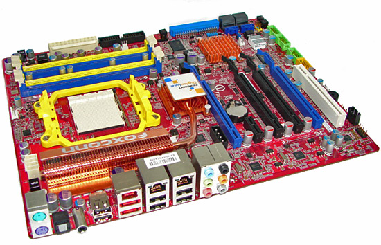
Foxconn sent us their new A79A-S motherboard that is part of their Digital Life series of products. This motherboard was not designed to be an extreme overclocker, but instead a feature rich platform that offers the capability to overclock when required. In testing to date, the board has actually gained a reputation of being an excellent overclocker along with a full featured BIOS. While the BIOS options are not as extensive as the top end 790FX products from ASUS or DFI, there are more than enough options to ensure successful overclocking for the vast majority of users. Foxconn is still developing the BIOS and we have sent our feedback on a few areas we would like to see improved, but overall, this board gets a recommendation from us.
We will take an additional look at the board during the official 790FX/SB750 launch activities next week but here are a few major features. The A79A-S includes four x16 PCIe 2.0 slots (dual x16 or quad x8 electrical), one PCIe x1 and one PCI slots, six native SATA II ports featuring RAID 0, 1, 5, or 10 support, two dual e-SATA ports, dual Gigabit LAN ports, Realtek ALC888 HD audio featuring DTS Connect and Dolby Digital Live support, 12 USB 2.0 connections, dual IEEE-1394a connections, LED Debug display, and on/Off/CMOS buttons.
Let's take a look at how all of this works, at least what we know works.


48 Comments
View All Comments
Maroon - Thursday, July 24, 2008 - link
"We can't help but wonder if it is because AMD is going a little too far in the sacrifices it's willing to make in the quest for higher clock speeds." Hello? This is the one thing that keeps the latest generation AMD procs from being competitive with Intel's. Are we sacrificing stability that you're not telling us?And then the bitching about the integrated LAN...please? Sounds like you guys are just pissed that AMD won't tell you the new SB works.
ughtas - Thursday, July 24, 2008 - link
I remember from months ago, that the L2/L3 cache performance was changed to support larger cache sizes. Is it possible that the tweaks that ACC makes to the processor timing improve the cycle time or allow better lookahead?nubie - Thursday, July 24, 2008 - link
I for one am glad to see an AMD processor at 3.4ghz, if this is a new trend I am all for it.I want to know what kind of clock-for-clock performance this has compared to an Intel, just for kicks.
I had a chat with a knowledgable IT guy, he claims that Intel systems boot faster to a usable desktop than AMD, and he has side by side bench tested them.
I didn't think to ask if he had done tests with comparable level 2 cache, an area that I think may be causing problems, AMD has no processors with 1M level 2 cache except a few older 90nm cores. They are just giving up in this area to Intel.
I applaud them for making neat server processors, but 512k level 2 cache is not cutting it these days.
I have been running on a Core2 "solo" Celeron 430 @2.4ghz for the last several months, and I must say while it is pretty damn fast there are times when it seems to "lock" or "micro-freeze" when it is doing a lot of multitasking.
Xray1 - Thursday, July 24, 2008 - link
Na, the L2 cache is pretty unimportant for AMD processors, as the on chip memory controller is very fast. For example, the difference between 1M L2 and 512k L2 K8 processors at otherwise same speed is for most apps somewhere in the range of 0-5%.Your single core Celeron locks in multitasking, because its single core.....single core is completely obsolete these days.
As to the boot speed: This heavily depends on the system config, bios etc. Plus: How often do you boot? I do that once a day and don't really care if it takes 30 sek more or less.
Xray1 - Thursday, July 24, 2008 - link
One reason for the proprietary 6pin connection between SB and CPU could be: It's simply a hardware dongle to ensure the best possible oc results can only be found on AMD chipset mainboards......It is very hard to believe AMD could not have made the same thing possible by MSR programming in the CPU.If AMD does not get more specific on this, we need true hardware nerds to sniff on these 6 lines and try to reverse engineer what's happening on them.
pmonti80 - Thursday, July 24, 2008 - link
Not so fast my friend.Just look here:
http://www.overclockers.com/tips01369">http://www.overclockers.com/tips01369
Now we have a more plausible explanation that does not involve strange "black magic".
ACC is just another form of CPU skew.
No big deal for anyone, end of the story.
ZootyGray - Friday, July 25, 2008 - link
Your linked source is not saying what you are saying. It's a guess. and conclusions are stated as being based on the assumption that the guesses and assumtions are true.Your attitude overrides that - NOT END OF STORY. And the results reported here stand untouched by your opinion based on what someone else said is assumption and guess. (right or wrong).
Additionally the author of your referenced article is very gracious in excusing himself if his guesses and assumptions are incorrect. And yet he ungraciously comes down pretty heavy in ending his article. And that is what has triggered your own feigned knowledgeable statement.
Maybe it is true - and maybe not. But oclokrs must live in perpetual embarrassment if it is true - and you embarrass yourself in the face of hard testing and accurate reporting of results of that testing. If I wanted speculative guessing and assumption and self agrandisement based on possibly erroneous opinion, I would go read bullshit at toms bubblegum guide. You might enjoy that more since you are apparently so inclined.
You put 60 hours work behind your statement and you might understand a cheap slap.
pmonti80 - Friday, July 25, 2008 - link
You are right on my attitude about last post. Sorry about that.But still I think the analysis of what could be happening here (based on both articles) is probably more in the line of CPU skew or some similar thing. It seems way easier to do with just 6 pins (4 or 5 really usable for ACC).
ZootyGray - Friday, July 25, 2008 - link
I agree with you. And it seems plausible (at least) that skew is quite probably it. The report however is about facts and not /guess /assumption /opinion - and therein is it's value.I fully expect that some will hack into this secret - much like was done before with AMD cpu's when they used the graphite pencil trix - it was all great.
Perhaps I owe an apology to you. I am a little overzealous since I have been seeking a factual, scientific review/testing site for some time. I like what's happening here. I hope I did not come down too heavily on you and the useful info that you presented. (altho the 'embarrass' part in that info,is merely abuse and useless shaming - essentially the stuff of flamewar, ego and fear (which reflects on the author).
Your point is taken and thank you for your (this) reply.
Xray1 - Friday, July 25, 2008 - link
The possibility that it is all about cpu skew/timings does not contradict what I have said. Why do you need a 6 pin connection from a southbridge to the CPU to change these settings? You can do that with simple register programming (MSRs). That's just like what has been done in the past (especially in timing settings of the AthlonXP FSB).So for me the big secret 6pin connection still looks like a big hardware dongle to allow for AMDs overclocking tool to only work on AMD chipset mainboards. They wanted to make it 100% non-software accessible, so there would be no way of doing it on non-AMD chipset boards. That's all I said. And yes, it's also speculation. But as long as they keep it cloed source, it's a non-accessible feature for other chipset makers.