NVIDIA's 1.4 Billion Transistor GPU: GT200 Arrives as the GeForce GTX 280 & 260
by Anand Lal Shimpi & Derek Wilson on June 16, 2008 9:00 AM EST- Posted in
- GPUs
Building NVIDIA's GT200
Here's a Streaming Processor, NVIDIA calls it an SP:
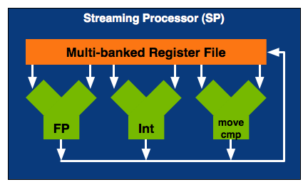
NVIDIA calls an individual SP a single processing core, which is actually true. It is a fully pipelined, single-issue, in-order microprocessor complete with two ALUs and a FPU. An SP doesn't have any cache, so it's not particularly great at anything other than cranking through tons of mathematical operations. Since an SP spends most of its time working on pixel or vertex data, the fact that it doesn't have a cache doesn't really matter. Aside from name similarities, one NVIDIA SP is a lot like a very simplified version of a SPE in the Cell microprocessor (or maybe the SPE is like a really simple version of one of NVIDIA's SMs, which we'll get to in a minute). While a single SPE in Cell has seven execution units, a single NVIDIA SP only has three.
By itself a SP is fairly useless, but NVIDIA builds GPUs and if you add up enough of these little monsters you can start to get something productive given that graphics rendering is a highly parallelizable task.
Here's a Streaming Multiprocessor, which NVIDIA abbreviates as SM:

A SM is an array of SPs, eight to be specific, along with two more processors called Special Function Units (SFUs). Each SFU has four FP multiply units which are used for transcendental operations (e.g. sin, cosin) and interpolation, the latter being used in some of the calculations for things like anisotropic texture filtering. Although NVIDIA isn't specific in saying so, we assume that each SFU is also a fully pipelined, single-issue, in-order microprocessor. There's a MT issue unit that dispatches instructions to all of the SPs and SFUs in the group.
In addition to the processor cores in a SM, there's a very small instruction cache, a read only data cache and a 16KB read/write shared memory. These cache sizes are kept purposefully small because unlike a conventional desktop microprocessor, the datasets we're trying to cache here are small. Each SP ends up working on an individual pixel and despite the move to 32-bit floating point values, there's only so much data associated with a single pixel. The 16KB memory is akin to Cell's local stores in that it's not a cache, but a software-managed data store so that latency is always predictable. With this many cores in a single SM, control and predictability and very important to making the whole thing work efficiently.
Take one more step back and you've got a Texture/Processor Cluster (TPC):
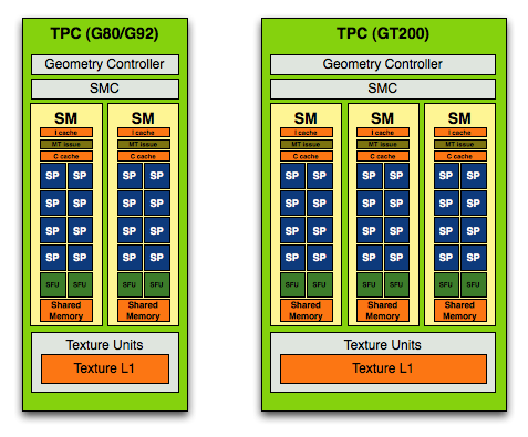
The G80/G92 TPC (left) vs. the GT200 TPC (right)
NVIDIA purposefully designed its GPU architecture to be modular, so a single TPC can be made up of any number of SMs. In the G80 architecture it was made up of two SMs but with the GT200 architecture it now has three SMs.
The components of the TPC however haven't changed; a TPC is made up of SMs, some control logic and a texture block. Remember that a SM is a total of 8 SPs and 2 SFUs, so that brings the total up to 24 SPs and 6 SFUs (must...not...type...STFU) per cluster in GT200 (up from 16 SPs and 4 SFUs in G80). The texture block includes texture addressing and filtering logic as well as a L1 texture cache.
The modular theme continues with the Streaming Processor Array (SPA) that is composed of a number of TPCs:
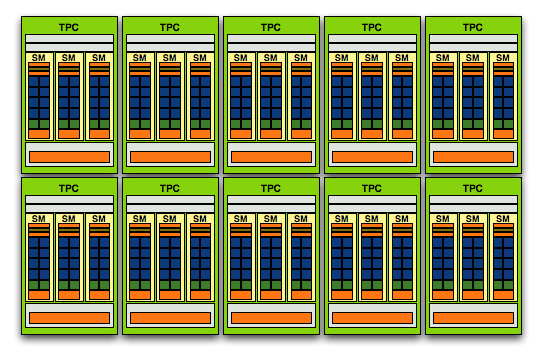
The GT200 SPA, that's 240 SPs in there if you want to count them
In G80 the SPA was made up of 8 TPCs, but with GT200 we've moved up to 10. Note that each TPC now has 3 SMs vs. 2, so the overall processing power of GT200 has increased by 87.5% over G80.
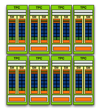
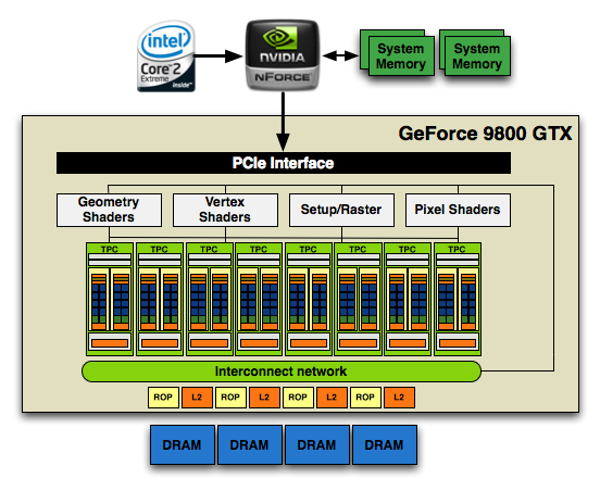
And here's G80/G92, only 128 SPs thanks to two SMs per TPC and 8 TPCs
At the front end of the GPU we've got schedulers and control logic to distribute workloads to the entire array of processing cores. At the other end we've got L2 texture caches and rasterization processors that handle final filtering and output of data to the frame buffer.
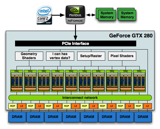
The culmination of all of this is that the new GT200 GPU, the heart of the GeForce GTX 280 and 260, features 240 SPs, 160KB of local memory, an even smaller amount of cache and is built on TSMC's 65nm process using 1.4 billion transistors.
1.4 Billion Transistors. It wants vertex data. Really bad.
754 Million Transistors
There are more transistors in this chip than there are people in China, and it's the largest, most compute-dense chip we've ever reviewed.


108 Comments
View All Comments
junkmonk - Monday, June 16, 2008 - link
I can has vertex data? LMFAO, hahha that was a good laugh.PrinceGaz - Monday, June 16, 2008 - link
When I looked at that, I assumed it must be a non-native English speaker who put that in the block. I'm still not entirely sure what it was trying to convey other than that the core will need to be fed with lots of vertices to keep it busy.Spoelie - Tuesday, June 17, 2008 - link
http://icanhascheezburger.com/">http://icanhascheezburger.com/http://icanhascheezburger.com/tag/cheezburger/">http://icanhascheezburger.com/tag/cheezburger/
chizow - Monday, June 16, 2008 - link
Its going to take some time to digest it all, but you two have done it again with a massive but highly readable write-up of a new complex microchip. You guys are still the best at what you do, but a few points I wanted to make:1) THANK YOU for the clock-for-clock comparo with G80. I haven't fully digested the results, but I disagree with your high-low increase thresholds being dependent on solely TMU and SP. You don't mention GT200 has 33% more ROP as well which I think was the most important addition to GT200.
2) The SP pipeline discussion was very interesting, I read through 3/4 of it and glanced over the last few paragraphs and it didn't seem like you really concluded the discussion by drawing on the relevance of NV's pipeline design. Is that why NV's SPs are so much better than ATI's, and why they perform so well compared to deep piped traditional CPUs? What I gathered was that NV's pipeline isn't nearly as rigid or static as traditional pipelines, meaning they're more efficient and less dependent on other data in the pipe.
3) I could've lived without the DX10.1 discussion and more hints at some DX10.1 AC/TWIMTBP conspiracy. You hinted at the main reason NV wouldn't include DX10.1 on this generation (ROI) then discount it in the same breath and make the leap to conspiracy theory. There's no doubt NV is throwing around market share/marketing muscle to make 10.1 irrelevant but does that come as any surprise if their best interest is maximizing ROI and their current gen parts already outperform the competition without DX10.1?
4) CPU bottlenecking seems to be a major issue in this high-end of GPUs with the X2/SLI solutions and now GT200 single-GPUs. I noticed this in a few of the other reviews where FPS results were flattening out at even 16x12 and 19x12 resolutions with 4GHz C2D/Qs. You'll even see it in a few of your benches at those higher (16/19x12) resolutions in QW:ET and even COD4 and those were with 4x AA. I'm sure the results would be very close to flat without AA.
That's all I can think of for now, but again another great job. I'll be reading/referencing it for the next few days I'm sure. Thanks again!
OccamsAftershave - Monday, June 16, 2008 - link
"If NVIDIA put the time in (or enlisted help) to make CUDA an ANSI or ISO standard extention to a programming language, we would could really start to get excited."Open standards are coming. For example, see Apple's OpenCL, coming in their next OS release.
http://news.yahoo.com/s/nf/20080612/bs_nf/60250">http://news.yahoo.com/s/nf/20080612/bs_nf/60250
ltcommanderdata - Monday, June 16, 2008 - link
At least AMD seems to be moving toward standardizing their GPGPU support.http://www.amd.com/us-en/Corporate/VirtualPressRoo...">http://www.amd.com/us-en/Corporate/VirtualPressRoo...
AMD has officially joined Apple's OpenCL initiative under the Khronos Compute Working Group.
Truthfully, with nVidia's statements about working with Apple on CUDA in the days leading up to WWDC, nVidia is probably on board with OpenCL too. It's just that their marketing people probably want to stick with their own CUDA branding for now, especially for the GT200 launch.
Oh, and with AMD's launch of the FireStream 9250, I don't suppose we could see benchmarks of it against the new Tesla?
paydirt - Monday, June 16, 2008 - link
tons of people reading this article and thinking "well, performance per cost, it's underwhelming (as a gaming graphics card)." What people are missing is that GPUs are quickly becoming the new supercomputers.ScythedBlade - Monday, June 16, 2008 - link
Lol ... anyone else catch that?Griswold - Monday, June 16, 2008 - link
Too expensive, too power hungry and according to other reviews, too loud for too little gain.The GT200 could become Nvidias R600.
Bring it on AMD, this is your big chance!
mczak - Monday, June 16, 2008 - link
G92 does not have 6 rop partitions - only 4 (this is also wrong in the diagram). Only G80 had 6.And please correct that history rewriting - that the FX failed against radeon 9700 had NOTHING to do with the "powerful compute core" vs. the high bandwidth (ok the high bandwidth did help), in fact quite the opposite - it was slow because the "powerful compute core" was wimpy compared to the r300 core. It definitely had a lot more flexibility but the compute throughput simply was more or less nonexistent, unless you used it with pre-ps20 shaders (where it could use its fx12 texture combiners).