NVIDIA's 1.4 Billion Transistor GPU: GT200 Arrives as the GeForce GTX 280 & 260
by Anand Lal Shimpi & Derek Wilson on June 16, 2008 9:00 AM EST- Posted in
- GPUs
Tweaks and Enahancements in GT200
NVIDIA provided us with a list, other than the obvious addition of units and major enhancements in features and technology, of adjustments made from G80 to GT200. These less obvious changes are part of what makes this second generation Tesla architecture a well evolved G80. First up, here's a quick look at percent increases from G80 to GT200.
| NVIDIA Architecture Comparison | 8800 GTX | GTX 280 | % Increase |
| Cores | 128 | 240 | 87.5% |
| Texture | 64t/clk | 80t/clk | 25% |
| ROP Blend | 12p / clk | 32p / clk | 167% |
| Max Precision | fp32 | fp64 | |
| GFLOPs | 518 | 933 | 80% |
| FB Bandwidth | 86 GB/s | 142 GB/s | 65% |
| Texture Fill Rate | 37 GT/s | 48 GT/s | 29.7% |
| ROP Blend Rate | 7 GBL/s | 19 GBLs | 171% |
| PCI Express Bandwidth | 6.4 GB/s | 12.8GB/s | 100% |
| Video Decode | VP1 | VP2 |
Communication between the driver and the front-end hardware has been enhanced through changes to the communications protocol. These changes were designed to help facilitate more efficient data movement between the driver and the hardware. On G80/G92, the front-end could end up in contention with the "data assembler" (input assembler) when performing indexed primitive fetches and forced the hardware to run at less than full speed. This has been fixed with GT200 through some optimizations to the memory crossbar between the assembler and the frame buffer.
The post-transform cache size has been increased. This cache is used to hold transformed vertex and geometry data that is ready for the viewport clip/cull stage, and increasing the size of it has resulted in faster communication and fewer pipeline stalls. Apparently setup rates are similar to G80 at up to one primative per clock, but feeding the setup engine is more efficient with a larger cache.
Z-Cull performance has been improved, while Early-Z rejection rates have increased due to the addition of more ROPs. Per ROP, GT200 can eliminate 32 pixles (or up to 256 samples with 8xAA) per clock.
The most vague improvement we have on the list is this one: "significant micro-architectural improvements in register allocation, instruction scheduling, and instruction issue." These are apparently the improvements that have enabled better "dual-issue" on GT200, but that's still rather vague as to what is actually different. It is mentioned that scheduling between the texture units and SMs within a TPC has also been improved. Again, more detail would be appreciated, but it is at least worth noting that some work went into that area.
Register Files? Double Em!
Each of those itty-bitty SPs is a single-core microprocessor, and as such it has its own register file. As you may remember from our CPU architecture articles, registers are storage areas used to directly feed execution units in a CPU core. A processor's register file is its collection of registers and although we don't know the exact number that were in G80's SPs, we do know that the number has been doubled for GT200.
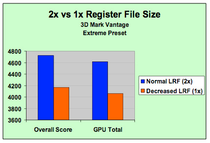
NVIDIA's own data shows a greater than 10% increase in performance due to the larger register file size (source: NVIDIA)
If NVIDIA is betting that games are going to continue to get more compute intensive, then register file usage should increase as well. More computations means more registers in use, which in turn means that there's a greater likelihood of running out of registers. If a processor runs out of registers, it needs to start swapping data out to much slower memory and performance suffers tremendously.
If you haven't gotten the impression that NVIDIA's GT200 is a compute workhorse, doubling the size of the register file per SP (multiply that by 240 SPs in the chip) should help drive the idea home.
Double the Precision, 1/8th the Performance
Another major feature of the GT200 GPU and cards based on it is support for hardware double precision floating point operations. Double precision FP operations are 64-bits wide vs. 32-bit for single precision FP operations.
Now the 240 SPs in GT200 are single-precision only, they simply can't accept 64-bit operations at all. In order to add hardware level double precision NVIDIA actually includes one double precision unit per shading multiprocessor, for a total of 30 double precision units across the entire chip.
The ratio of double precision to single precision hardware in GT200 is ridiculously low, to the point that it's mostly useless for graphics rasterization. It is however, useful for scientific computing and other GPGPU applications.
It's unlikely that 3D games will make use of double precision FP extensively, especially given that 8-bit integer and 16-bit floating point are still used in many shader programs today. If anything, we'll see the use of DP FP operations in geometry and vertex operations first, before we ever need that sort of precision for color - much like how the transition to single precision FP started first in vertex shaders before eventually gaining support throughout the 3D pipeline.
Geometry Wars
ATI's R600 is alright at geometry shading. So is RV670. G80 didn't really keep up in this area. Of course, games haven't really made extensive use of geometry shaders because neither AMD nor NVIDIA offered compelling performance and other techniques made more efficient use of the hardware. This has worked out well for NVIDIA so far, but they couldn't ignore the issue forever.
GT200 has enhanced geometry shading support over G80 and is now on par with what we wish we had seen last year. We can't fault NVIDIA too much as with such divergent new features they had to try and predict the usage models that developers might be interested in years in advance. Now that we are here and can see what developers want to do with geometry shading, it makes sense to enhance the hardware in ways that support these efforts.
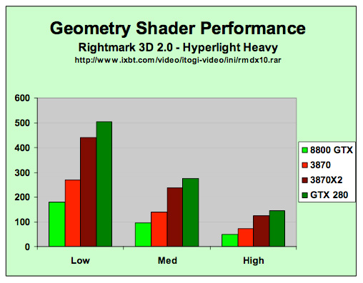
GT200 has significantly improved geometry shader performance compared to G80 (source: NVIDIA)
Generation of vertex data is a particularly weak part of NVIDIA's G80, so GT200 is capable of streaming out 6x the data of G80. Of course there are the scheduling enhancements that affect everything, but it is unclear as to whether NVIDIA did anything beyond increasing the size of their internal output buffers by 6x in order to enhance their geometry shading capability. Certainly this was lacking previously, but hopefully this will make heavy use of the geometry shader something developers are both interested in and can take advantage of.


108 Comments
View All Comments
skiboysteve - Tuesday, June 17, 2008 - link
FANTASTIC write up on fine-grained TMT. I was unaware about this threading technique and was always thinking of this in class or whenever someone would talk about hyperthreading. this technique was literaly in my head for well over a year and I didn't know what it was called or that it even had a name. I always thought there had to be a more elegant way than hyperthreading to do multithreading down at the chip level without doing the OS style time slicing.i was sitting there wondering how the hell the schedule and run these SPs and then bam whole page about it
really appreciate the effort that goes into researching the core of these chips. i know not everyone likes it but for guys that are educated and work in the field its really interesting
DerekWilson - Tuesday, June 17, 2008 - link
remember though that this type of fine-grained TMT only has payoffs in systems running millions of threads concurrently.on an OS you'll see hundreds or even thousands of threads on heavily used systems, but there still wouldn't be enough concurrent action to justify this type of architecture for general purpose computing.
of course, as developers push towards an effort to thread their code as much as possible, who knows what architectures might be worth exploring on the desktop ...
coder0000 - Tuesday, June 17, 2008 - link
Very well written! A couple of points:1) Last week at WWDC Apple announced OpenCL as an alternative to CUDA. It's a C99 based HLL for creating compute kernels that can be deployed to GPU's and CPU's. Today Khronos officially announced a working group for this, and NV is a part of the committee. As such, your wish for an industry standardized compute language similar to CUDA that runs on all platforms and vendors HW may not be so far off.
2) I believe your interpretation of how multiple threads simultaneously execute in an SM is incorrect. Per thread context switching is not free, and you would never be able to execute a different thread every cycle in the manner described. There is far too much context that needs to be swapped out, and there would be significant power implications for doing that, in addition to the latency. Instead, I believe what NV is claiming is that any given SP executes a single thread. All threads in the SM can all be a single warp, but you can also have multiple threads (one per SP) all executing simultaneously in an SM.
DerekWilson - Tuesday, June 17, 2008 - link
1) I haven't had a good chance to look at OpenCL, but I certainly hope that if it's everything everyone is saying it is in the comments here that it takes off in a bigger way than CUDA :-)2) it does not context switch per thread -- warps define a context, and you have 32 threads grouped together. these threads all share the same instruction stream, which is why if threads in a warp take different directions on a branch all 32 threds must follow both paths.
NVIDIA has flat out stated that every schedule clock a new warp is scheduled and that it takes 4 clock cycles to process one warp on an SM. For both of these to be true, we conclude that the scheduler alternates scheduling SPs and SFUs on altenating clocks which means the SPs would be scheduled every 4 clocks relative to itself.
On 8 SPs per SM, you some how need to execute 32 threads in 4 clock cycles. This makes sense if you execute 4 threads per SP in some way. The details at this point are fuzzy though.
regardless, if an SP executes 4 different threads from the same warp, there is no need to context switch to execute any of these threads -- again, threads in the same warp share context.
skiboysteve - Tuesday, June 17, 2008 - link
could be a large explanation of the 2x register file size. and remember that the SP doesn't have to worry about the context switch, the SM handles having the data in the right placeanandtech02148 - Monday, June 16, 2008 - link
From this conclusion, Amd seems to be the shrewd player, let nvidia and intel duke it out in the high voltage, heat, meaningless speed gpu while Amd can pull something like its first dualcore or athlon64 for the win.this new beast from Nvidia will have how many developers making games for it right away? i'm guestimating maybe 2yrs-4yrs down the road we'll see a decent title that take full advantage of this hardware.
by then Amd will have something of a midrange that can more than handle the games.
2 things nvidia could work on that it already has, the ps3 market, and small graphic devices to improve profits. shrink the ps3 gpu further so Sony can shrink it's machinel and sell more.
PrinceGaz - Monday, June 16, 2008 - link
The GT200 core may be a technical masterpeice in terms of actually making something that big which is fully functional on GTX280 cards, but it seems to me the penalty of fabbing it at 65nm negates much of the benefits of such a wide GPU.They've had to drop the clock speeds throughout presumably because of the ridiculous amount of heat such a large core generates, which means the ~60% performance advantage in current games over the G80 core at similar clock-speeds is somewhat reduced.
Given that ATI are not producing their 55nm cores in AMD's fabs but instead are getting them churned out reliably elsewhere, nVidia have made a mistake this time around in having their high-end product rely on previous-generation fabrication as it makes it run too hot to allow the clock-speeds needed for it to be the product it should be. There is always a risk in transitioning to a smaller fab technology, and nVidia suffered badly in the past by doing so too early, but with a chip the size of the GT200, they really should have gone to 55nm even if it meant a delay of a month or three, whilst the smaller cut-down derivatives were rolled out first.
ekpyr - Monday, June 16, 2008 - link
Great article, but what about the microstuttering issues present in Nvidia's 9800GX2 cards (both SLI and Quad-SLI)? There is very little discussion on this, but I've seen some benchmarks where the FPS floor is 4fps with the 9800GX2s. Can you add a subjective review of whether or not the actual gameplay is smoother with the GTX280s across these games? Aggregate numbers may say one thing, but I've returned a 9800 GX2 Quad-SLI setup because it was unable to handle the incredible amount of texture loading that was done in Age of Conan (2560x1600 4xAA 'High' settings = 4fps). The 8800 GTX Tri-SLI configuration I am currently using is more resilient to microstuttering with its increased bus and memory capacities, but I'm very curious about the GTX280s and their increased memory and bus on texture-heavy games like Age of Conan.DerekWilson - Monday, June 16, 2008 - link
the only game that came close to having this issue with quad sli for us was oblivion.in that game at high res lag and stutter are unbearable and the game is unplayable.
we didn't notice any stuttering issues with a single GX2.
i'm working on some analysis tools to show details like this better in future articles.
TheJian - Monday, June 16, 2008 - link
I find it humorous that nobody discusses the fact that the shrink has already taped out and will likely be out in two months or just after. This humongous chip was only released so that when AMD releases in the next few weeks they will be behind still in single GPU cards. This is basically what Intel does to AMD every time AMD has a better chip. For all intents and purposes this is a PAPER release of what will come in 2-2.5 months (In Intel's case they just show you what will be out 6 months from now, and a large portion of people don't buy an AMD because Intel might be ahead by xmas...LOL - works like a charm every time AMD is ahead). THE DIE SHRUNK CHIP! Most likely with faster speeds. I suspect they'll come with "ULTRA" version first (and stick it on top of the price heap, so as to not kill all FAT cards in the channel already) and then filter down as these big suckers leave the channel. That's if they even plan to sell more than a few of these to begin withat 65nm. It's only out there so AMD won't look any good in two weeks.MIND SHARE is everything, which is why Intel's KING of the paper launch when behind strategy. They've even went to doing it for all chips no matter what now. Nehalem scores 6 months before availability. AMD's marketers have no clue an should be fired. You have to play the same DIRTY game as your enemy or you've already lost. If AMD had half a brain in their head they'd paper launch an ultra or 2x4870 version for the same reason...LOL. Then claim "our 4870x2 makes nvidia look like crap for $600"...ROFL. Who cares when it's available, just say it. Having said that, Nvidia will wipe the floor with them in 2 months anyway on a 2xGTX280 that's die shrunk. Which is all they are doing today...BUYING TIME!