NVIDIA's 1.4 Billion Transistor GPU: GT200 Arrives as the GeForce GTX 280 & 260
by Anand Lal Shimpi & Derek Wilson on June 16, 2008 9:00 AM EST- Posted in
- GPUs
Derek Gets Technical: 15th Century Loom Technology Makes a Comeback
Because it's multithreaded...
Yes I know it's horrible, but NVIDIA has gone a bit deeper in explaining their architecture to us and they thought borrowing terminology from weaving was clever. But as much as that might make you want to roll your eyes, the explanation of how things work that is enabled is worth it.
In cloth weaving, a warp is the vertical group of parallel threads that are held taught while the weft are the threads passed through these. I suppose it makes sense, then, that NVIDIA decided to call their grouping of parallel threads to be executed on an SM a warp.

See the group of threads that hang from the top of this loom? That's called a warp.
With each SM having 8 SPs and G80 having two SMs per TPC (for a total of 16 SPs) it looked like a natural fit to execute quads across these 16 scalar units. We learned that this was not the case, but seeing the grouping of three SMs per TPC in GT200 still looked a little funny until we really learned more about how things are scheduled on NVIDIA's unified architecture. Each SM's scheduler picks a new warp to work on every clock cycle, and since the scheduler runs at half speed this ends up being every other clock cycle from the perspective of the rest of the SM. Each warp is made up of a group of 32 threads (in pixel shaders this is a group of 8 quads) that share an instruction stream (a shader program or a kernel if you're talking about GPU computing).
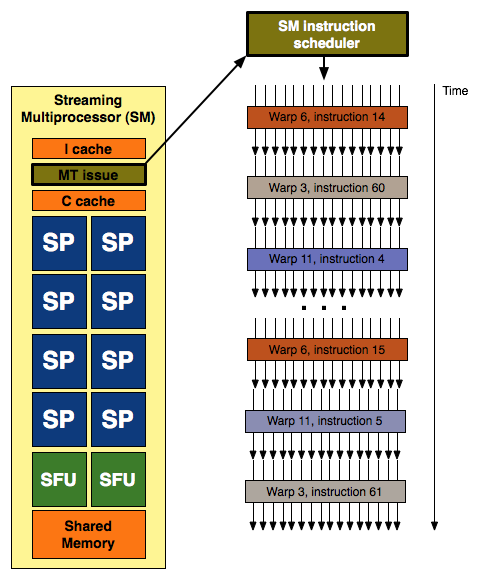
32 threads in a warp, issued in two groups of 16 threads - one such group is depicted above
Different warps built from threads executing the same shader program can follow completely independant paths down the code, but every thread within a warp must be exectuing the same instruction. This means that our branch granularity is 32 threads: every block of 32 threads (every warp) can branch independantly of all others, but if one or more threads within a warp branch in a different direction than the rest then every single thread in that warp must execute both code paths. Each threads only retains the result from the path it was supposed to follow probably by using the branch result to dynamically predicate the apporpriate path per thread. Each SM can have 32 (up from 24 in G80) warps in flight at the same time (for a total of 1024 threads in flight per SM). With 10 TPCs each containing 3 SMs, that's up to 30720 threads in flight on a GTX 280.
Each SM with it's 8 SPs and 2 SFUs is capable of processing up to 8 ops per clock (MAD (a fused floating point multiply and add) being the most complex) in the SPs and 8 ops per clock on the SFUs (which are made up of 4 floating point MUL units and other logic). Warps are executed on SMs in 2 groups of 16 threads (probably four quads for pixels) over four clock cycles.
This is where it gets interesting.
The SPs and SFUs are scheduled on alternating clock cycles from the perspective of the SM scheduler. They execute independent warps. SPs are scheduled on one clock cycle and SFUs are scheduled the next. Each is able to complete the processing of an entire warp before the next time it is scheduled, which happens to be four clocks (relative to the SPs and SFUs) after they it was scheduled with the last warp.
But wait ... aren't SMs supposed to be able to support dual-issue MAD+MUL? Well, back when G80 launched, Beyond3d did an excellent job of exploring the reality of the situation. With the fact that the SFU handles the "dual-issued" MUL and shares its time with other responsibilities like transcendental calculation and attribute interpolation, the ability of the hardware to actually accelerate cases that could take advantage of dual-issue was significantly reduced. But this scheduling revelation makes it clear that the problem is much more complex.
In order for code that could benefit from dual-issue hardware to take advantage of G80 or GT200, a warp must be scheduled on an SP for the MAD and then it must be re-scheduled on the SFU before it hits the SPs again. If the SFU is too busy handling attribute interpolation or transcendental math, then our warp will be rescheduled on the SPs to calculate the MUL and we will have lost our potential dual-issue speed up.
NVIDIA tells us that they "had some scheduling/issue problems with getting the MUL in the SFU to work consistently per clock. We fixed that in GT200." This makes perfect sense in light of what we now know about scheduling on G80/GT200. What they needed to do to improve the ability of their hardware to speed up cases where a MAD+MUL dual issue would help was to make sure that these cases were properly prioritized to execute on the SFU. We don't see MAD+MUL in every line of code, so giving these cases higher priority on the SFU than its other duties should help to optimize the utilization of the hardware. They do have to be careful not to start just running random MULs on the SFU because those special functions do still need to get done, but pushing a select subset of MULs onto the SFU (where they directly follow MADs that have just been executed on SPs) should definitely help in certain cases.
Really the main focus for NVIDIA is proper utilization and prioritization. Everything for any given frame needs to get done at some point or other, so simulating "dual-issue" shouldn't take priority over other things that need to get done that might be more important to completing the next frame. But organizing how to handle it is a big deal. Real time compilers are a big part of that, but internal thread management and scheduling in an architechure this wide also cannot be ignored. NVIDIA says they can now get 93-94% efficiency from their "dual-issue" implementation in directed tests and that this is significantly higher than on G80. Real world results will be lower, but the thing to remember is that the goal is simply to make maximally efficient use of the hardware availalbe. Just because the SFU isn't assisting in a MAD+MUL every clock doesn't mean it isn't doing something important.
This whole situation leaves us with mixed feelings. The hardware itself is not capable of "dual-issue" as it is understood in an architectural sense. The obfuscation of graphics hardware technology in a competitive industry has been the norm for the past decade, and we can accept this. We would prefer to know what the hardware is actually doing, but we are more than happy to have an explanation of something as a hardware feature where the hardware merely simulates the effect a specific architectural design has. But in the case where the hardware doesn't perform in nearly the same way as it would if the feature had actually been implemented as a hardware feature, we just can't help but be a little disappointed.
And we are conflicted about this because NVIDIA's design is actually very elegant. Attribute interpolation will always need to be done, and having hardware set aside for complex math is also very useful. But rather than making a dedicated fixed function interpolator or doing taylor expansion of complex math on SPs, NVIDIA built hardware that could serve both purposes and that had time left over to help offload some well placed MULs within the instruction stream of running programs.
If NVIDIA had been as open about their architecture as Intel is about their CPU designs, we could not have helped but to be impressed by this. The "missing MUL" wouldn't have been seen as a problem with NVIDIA's dual-issue "hardware"; we would have been praising NVIDIA's ability to schedule and multitask the different units within their SMs in order to improve utilization.


108 Comments
View All Comments
woofermazing - Tuesday, June 17, 2008 - link
Isn't the R700 high-end model going to have a direct link between the two cores. Could be a false rumor, but i would think that would solve a lot of problems with having two GPU's on a single board, since games would see it as 1 chip instead of a Crossfire/SLI setup. And besides, why the heck does it matter what the card looks like under the cooler. If it delivers better performance than Nvidia's offering without driver headaches, I don't think most gamers are going to care.VooDooAddict - Tuesday, June 17, 2008 - link
Why am I the only one happy about this product?Since the release of the 8800GTX top end single GPU performance has been a little stagnant... then came the refresh (8800GT/8800GTS-512) better prices came into effect.
Now we've got the new generation, and like in years prior, the new gen single GPU card has near performance of the previous gen in SLI. Price is also similar with when NVIDIA launched the first 8800GTX.
Sure, I wish they came in at a lower price point and at less power draw. (Same complaints that we had with the original 8800GTX). Lower power and lower price will come with a refresh.
Will I be getting one? ... nahh these cheap 9600GTs, overclocked 8800GT's and 8800GTSs will be the cards I recomend till i see the refresh. But I'm still happy there's progress.
I'm hoping the refresh hits around the same time as Intel's updated quad core.
DerekWilson - Tuesday, June 17, 2008 - link
i think its neat and has very interesting technology under the hood.but i'm not gonna spend that much money for something that doesn't deliver enough value (or even performance) compared to other solutions that are available. you pretty much reflect my own sentiment there: it's another step forward but not one that you're gonna buy.
i think people "don't like it" because of that though. it just isn't worth it right now and that's certainly valid.
greenx - Tuesday, June 17, 2008 - link
There are two ways I can look at this article.1)First an foremost at the heart of a real gamer ticks the need for good story lines fed by characters you will never forget, held by a gameplay you will fall in love with and finally covered by graphics that will transport you to another world (kinda like when I first played FF VII on my PC).
Within the context of the world we live in today I wonder what is really going through the minds of these people selling $600+ video cards. Kinda like those $10 000+ PCs. Madness. Sure they have their market up there but I shudder to think of how much money has been poured into appeasing a select few. Furthermore for what reason? Glory? I don't know but seeing as how the average gamer is what has made the PC/Gaming scene what it is, where does a $600+ video card fit into the grand scheme of things?
2) The possibilities that these new cards open up certainly seem exciting. The comparison with intel has been justified, but considering the other alternatives out there are much further ahead in development, who is going to bypass intel/amd/etc for a GPU technology based supercomputer?
DerekWilson - Tuesday, June 17, 2008 - link
two address point 2):developers will bypass Intel, AMD, SUN, whoever owns Cray these days, and all other HPC developers when a technology comes along that can speed up their applications by two orders of magnitude immediately on hardware that costs thousands (and in large cases millions) less to build, run and develop for.
evolucion8 - Tuesday, June 17, 2008 - link
LOL that was quite funny but incorrect as well, there's more than 4 Billion of people in China, in the future probably nVidia will launch a 4 Billion Transistors GPU hehe. It will require a Nuclear Reactor to turn it on, a and two of them to play games :D7Enigma - Wednesday, June 18, 2008 - link
4 Billion? Did you just make that out of thin air. Latest tabs show approximately 1.4 billion (give or take a couple hundred million). The world population is only estimated at 6.6 billion, so unless 60% of the people in the world are living in China, you're clueless.http://geography.about.com/od/populationgeography/...">http://geography.about.com/od/populationgeography/...
Bahadir - Tuesday, June 17, 2008 - link
Firstly I must say I enjoyed reading the whole article written by Anand Lal Shimpi & Derek Wilson. However, what does not make sense to me is the fact that "At most, 105 NVIDIA GT200 die can be produced on a single 300mm 65nm wafer from TSMC", but by looking at the wafer, only 95 full dies can be seen. Is this the wrong die?Also, it is not fair to compare the die of the Penryn against the GTX 280die because Penryn's die was made in 45nm process and GTX280 was made in 65nm die. Maybe it would be fair to compare it with the Conroe (65nm) die. But well done folks for putting an excellent article together!
Anand Lal Shimpi - Tuesday, June 17, 2008 - link
Thanks for your kind words btw :) Both of us really appreciate it - same to everyone else in this thread, thanks for making a ridiculously long couple of weeks (and a VERY long night) worth it :)-A
Anand Lal Shimpi - Tuesday, June 17, 2008 - link
You're right, there's actually a maximum of 94 usable die per wafer :)Take care,
Anand