Intel's Atom Architecture: The Journey Begins
by Anand Lal Shimpi on April 2, 2008 12:05 AM EST- Posted in
- CPUs
A Prelude to Success
This all started back in 2004, in Austin, Texas. Despite the location, I am talking about Intel and not AMD. In 2004, Intel's Austin Design Center was hard at work on another member of the Pentium 4 processor family - codenamed Tejas.
Tejas was scheduled to arrive after Prescott and continue the NetBurst lineage, but as history would have it, Tejas never saw the light of day. The project was canceled and Intel's corporate attention was instead shifted to taking the Pentium M architecture and improving it to be desktop-worthy.
The Tejas team was, as you'd expect, not particularly pleased with their project being canceled. But, as seems to be the case with Intel's best engineers and canceled projects, they channeled their disappointment into passion and excitement for their next design.
I should stop the story here and point out the striking similarity to another Intel success story, that of the original Centrino. Banias was the first Centrino processor, later named the Pentium M. The team that worked on Banias was the same team that worked on Timna, yet another project cancelled very late in the process. After Timna was cancelled the team, working out of Intel's Israel Design Center, went into a brief collective depression for about a month before receiving instructions to work on Banias. Instead of producing something mediocre, the team felt a need to prove something to those who cancelled their beloved Timna project. The result was Banias, which became the Pentium M, led to the Core Duo and eventually gave us the Core 2 family of processors that we love so dearly today.
Back to Austin. We've got a very small team of people who were hard at work on Tejas and now without anything to do. The same sense of proving their worth brew and in 2004 the team received new orders.
The task was to develop a low power, IA (Intel Architecture, read: x86) core for use in a many-core CPU design. Since this core would be used in a many-core CPU, it would have to be very, very low power (you can't have 10s of cores each consuming 100W).
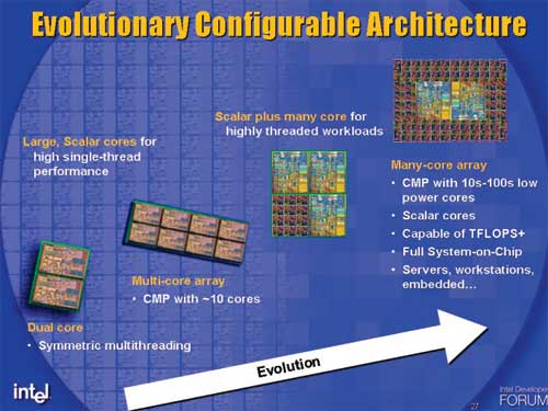
Many-core CPU designs are in Intel's future, Atom has its roots in the many-core initiative
I asked the design team in Austin if this was a dirty joke played on them by upper management - going from a very power hungry design like Tejas to something that would consume a couple of watts. Apparently during Tejas' design, a smaller team in Austin was doing some pathfinding work, looking at very low power simple cores. Since they spent about a year doing this pathfinding work, the transition from Tejas to something very low power was natural despite what it may seem from the outside.
Many of the architects that would work on this new, low power core actually came from other microprocessor companies. Belli Kuttanna, the chief architect on the core, worked for Sun on SPARC processors as well as Motorola designing elements of PowerPC cores. Belli worked with others from Sun and Motorola, but now all under the Intel umbrella. One of the members of the validation team working on the core was also a former AMDer.
Early 2004 was the inception of the pathfinding effort to investigate what would be necessary to develop this new low power core. The codename for this core was Bonnell, which as I've mentioned before is the tallest mountain in Austin, measuring only 750 ft. The petite mountain was a perfect fit for this new, small core (engineers aren't the most creative with naming ;)).
The first step in the pathfinding effort was to find out if Bonnell could be based on an existing Intel microarchitecture. The small team looked at reusing the Pentium M or the yet-to-be-released Core 2 and some analysis was done on both of these options. It didn't take long to come to the conclusion that it wasn't possible to hit the power and performance targets using an existing design. As Intel discovered with Centrino, in order to target a new market it would need to use a new microprocessor design.
The team went back to a clean sheet of paper and started with the simplest of microprocessor architectures, a single-issue, in-order core and built up from there. The designers kept iterating until the performance and power targets at that time were met. You have to keep in mind that in 2004, even Intel didn't have a good idea of exactly where this core would be used. Imagine going back to 2004 and being expected to design the microprocessor architecture that could eventually be used in something like a third generation iPhone - it's borderline impossible.
By the end of 2004, Paul Otellini gave the Austin team specific direction that the Bonnell core would be used in a standalone CPU - not as a part of a many-core design effort. This CPU would be used in UMPCs (Ultra Mobile PCs) and an even more unheard of creation called a MID (Mobile Internet Device). The many-core designs are still under development and I suspect that the first one we'll see come to fruition is a little gem called Larrabee.
Bonnell was just a core, but when combined with a L2 cache and an external bus interface it became the CPU known internally as Silverthorne. More recently, Intel gave Silverthorne a proper name and called it the Atom processor.


46 Comments
View All Comments
highlandsun - Thursday, April 3, 2008 - link
With all due respect to Fred Weber, with Atom at 47 million transistors, it's pretty obvious that the 10% figure for X86 ISA compatibility is not negligible, particularly in this performance-at-absolute-minimum-power space. Anybody using X86 in tiny embedded systems is automatically giving up a chunk of their power budget that someone using a cleaner instruction set encoding can apply directly to useful work. And as the previous poster already pointed out - source code portability is the only thing that matters to application developers, and that's a non-problem these days. Using the X86 instruction set encoding is stupid. Using it on a low-power-budget device is suicide.Jovec - Thursday, April 3, 2008 - link
I don't think the 10% reference meant 10% of all chips, but rather 10% of the current chip at the time the statement was made. In other words, x86 instruction decoding requires (roughly) a fixed amount of transistors for any chip, so the smaller the die size and larger the transistor count, less and less space is devoted to it.highlandsun - Thursday, April 3, 2008 - link
Yes, that's obvious. And it's also obvious that Atom at 47 million transistors is paying a greater proportionate cost than Core2 Duo at 410 million transistors. In 2002 when Fred made that statement, AMD's current chip was the AthlonXP Thoroughbred, with about 37 million transistors. At the same time the Pentium 4 had 55 million. Put in context, I'd guess that the Atom at 47M vs P4 at 55M has more than 10% of its resources devoted to X86 decoding.Also, Fred's statement in 2002 didn't take into account the additional complexity introduced by the AMD64 instruction extensions, where now a single instruction may be anywhere from 1 to 16 bytes long. Given that you're doing a completely clean ground-up chip design in the first place, it would have made more sense (from both a power budget and real estate perspective) to design a clean, orthogonal, uniform-length encoding at the same time.
Cross-platform ABI compatibility is stupid in the context they're aiming for; nobody is going to run their PC version of Crysis or MSWord on their cellphone. All that matters is API compatibility. With a consistent API, you can still run a separate binary translator if you really really want to move a desktop app to your mobile device but in most cases it would be a bad idea because a desktop app is unlikely to take advantage of power-saving APIs that would be important on a mobile. I.e., most of the time you're going to want purpose-built mobile apps anyway.
floxem - Tuesday, April 15, 2008 - link
I agree. But it's Intel. What do you expect?maree - Thursday, April 3, 2008 - link
I dont think MS will be ready before Windows 7 is released, which is another 3-5 years... and might coincide with Moorestown. Microsoft started work on WindowsLite only after releasing Vista. Vista is bloatware as of now. As of now MS has to rely on crippled versions of XP and Vista like starter and home, which is not very ideal.Apple and Linux are going to have a free run till then...
TA152H - Wednesday, April 2, 2008 - link
Bringing up the Pentium is a little strange, because the whole market is completely different.The Pentium wasn't supposed to be for everyone when it came out. The processor market was different back then where previous generations lasted a long, long time. The Pentium wasn't supposed to replace the 486 right away, or even quickly, and being huge and a terrible power hog was acceptable because the initial iteration was just for a very small group of people who absolutely needed it. The original Pentium had a lot of problems, and struggled badly to reach 66 MHz, so they sold most of their processors at 60 MHz. The second generation was intended more for mainstream.
Nowadays the latest generation replaces the earlier much more quickly, and has to cover more market segments more quickly. I still remember IBM releasing new machines for the 8086 in 1987. That's 9 years after the chip was made. It's just a different market.
The Pentium is nothing like the Silverthorne though, and it's a strange comparison. The Pentium executed x86 instructions, it wasn't decoupled. It also had both pipes, the U and V, lockstepped, which is limitation the Silverthorne doesn't have.
Saying the Pentium Pro was the first processor that allowed out of order processing is strange indeed. The only other processor this would have made sense with was the Pentium, since it was the only previous processor that was superscalar. So, they only made one in order processor, and then went to out of order with the next. It's difficult to see the extrapolation from this that it will be five years or more before Silverthorne goes out of order. It might be that long, but the backwards reference shouldn't be used to back that; it does more to contradict it.
Anand Lal Shimpi - Wednesday, April 2, 2008 - link
The Pentium reference was merely to show that what was once a huge, 300mm^2 design could now be built on a much, much smaller scale. And starting from scratch it's now possible to build something in-order that's significantly faster.The Pentium was an obvious comparison given that it was Intel's last two-issue in-order design, but I didn't mean to imply anything beyond that.
It won't be too long before we'll be able to have something the speed of a Core 2 in a similarly small/cool running package as well :)
Take care,
Anand
fitten - Wednesday, April 2, 2008 - link
I remember back in the days of the Mac FX we talked about 'what ifs' like making a 6502 with the (then) modern process technologies and how fast would it run. I wonder what about now :)crimson117 - Wednesday, April 2, 2008 - link
I am SO going to hold you to that! But I can only hope "won't be long" will mean within 12 months rather than within 12 years :P
Especially after my fiasco mounting a Freezer 7 Pro on an Abit IP35-E, I'd love if a heatsink weren't even necessary.
Anand Lal Shimpi - Wednesday, April 2, 2008 - link
12 months won't be a reality unfortunately :) But look at it this way, the first Pentium M came out in 2003? And 5 years later we're able to have somewhat comparable performance with the Atom processor.I'm really curious to see what happens with Atom on 32nm...