Intel's Atom Architecture: The Journey Begins
by Anand Lal Shimpi on April 2, 2008 12:05 AM EST- Posted in
- CPUs
Building by FUBs
Below we have a conventional block diagram of the Intel Atom processor:
You'll see nine distinct blocks and in conventional microprocessor design at Intel, this is how the chip would be divided and conquered. You'd have one team working on the L2 cache, one team working on the IO interfaces, etc... Unfortunately the team at Austin was significantly smaller than your conventional microprocessor design group, so things had to be done a little differently.
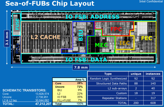
Intel calls the Atom approach a Sea-of-FUBs chip layout, a more granular approach to chip layout and design. A FUB (Functional Unit Block) is a floor-plannable object, an individual adder is a FUB, a decoder is a FUB, a cache is a FUB, etc... Because the size of each FUB made them more manageable, a single designer could handle multiple FUBs. The FUBs were also treated more modularly so that once a FUB was defined, designers can work on the FUB, chip integraters can give it to the layout guys and the timing guys can work in parallel as well. It allows for much more concurrent design than the conventional, more serial approach to chip design.
Approximately 90% of the fubs are built using standard Intel logic cells, minimizing the amount of custom work that needs to be done and decreasing the time to market on a processor like Atom. Minimizing the amount of custom Intel logic also means that it's easier to produce variants of Atom that may incorporate other important features depending on the target market.
The Sea-of-FUBs approach was also driven by a desire to keep power consumption and feature creep to a minimum. Area budgets were developed for each FUB and cluster of FUBs and Intel forced the designers to stick to these budgets. If a designer needed more die space for their FUB they couldn't just take it. A review board was setup where designers would come in and ask to grow their FUB. They were allowed to grow the FUB only if they were able to find another FUB that would shrink to accommodate it. The same thing applied for power.


46 Comments
View All Comments
adntaylor - Tuesday, April 8, 2008 - link
On that chart with price / power, you need to be clearer...For price, you show the combined price for CPU + Chipset. For power, you say just the CPU... so 0.65W for the CPU... but you're conveniently ignoring the >2W figure for the chipset!!! This absolutely flatters Intel wherever possible.
AMD are just as misleading - they describe the Geode LX as "1W" which excludes the non-CPU core parts of the chip (which is an integrated CPU + GMCH)
Just please be honest - the figures are out there in the Intel datasheets... it takes 10 minutes to check.
Clauzii - Friday, April 4, 2008 - link
I still have a PowerVR 4MB addon card, runnung in tandem with a Rage128Pro. Quite a combination w. 15 FPS in Tombraider. Constant(!) 15FPS, that is..Amazing what they actually achieved back in 95!
Clauzii - Friday, April 4, 2008 - link
Ooops!Totally misplaced that. Sorry.
wimaxltepro - Friday, April 4, 2008 - link
The Atom represents a shift in processor architecture that is the most dramatic departure for Intel since introduction of x86 processors... the philosophy of how computing itself occurs from centralized processors to distributed processing based on an extension of the popular x86 instruction set.The Atom is not about the immediate prospects for the Atom or Nehalem products: we will likely see members of Intel's new product family be used in embedded applications in consumer products and in areas where specialized communications processors are more the rule. While not optimized for use in specific networking applications, the products capitalize on the wide range of support available in IT/Networking to develop common functions that leverage the low cost, low power/processing capability to be used as a common denominator for a wide range of applications.
Intel has been built on the 'Wintel' architecture: massively integrated chips needed to handle the massively integrated operating systems and applications of Windows (and Apple) environments. The Atom allows migration and broadening out from that architectural motif to a very highly distributed architecture. So, the increased parallelism found in the internal chip architecture is enabling of changes in external system architectures and device applications that go well beyond the typical domain of Intel.. and right into the domain of 'personal wireless broadband' and SDWN, Smart Distributed Wireless broadband Network.
The decisions about in-order vs. out of-order instruction streams, memory architecture, I/O architecture have been made in light of the broad vision for how computing, networking and, out of hand, how wireless enabled broadband networking including WiMAX will occur. This should be understood for what it represents as a shift in direction for Intel both in response to broad industry shifts and as a trend setting development.
jtleon - Friday, April 4, 2008 - link
Thanks to all the flash player ads, etc., a mobile web device will continuously avoid switching to low power states. Thus one could argue that advertising will be carbon footprint enemy of the internet's future. This is already becoming the case for desktop/laptop machines.Without such continuous (arguably wasted) consumption of CPU power, then Intel's engineered power management might have a significant impact on the value of the Atom.
Regards,
jtleon
0WaxMan0 - Friday, April 4, 2008 - link
I am definatly much impressed and enthused by intels work here, the future looks interesting esp for those of us who like low power cross compatible computing products.However I have to point out that a low power modern x86 cpu has allready been done infact 4 years ago with AMD's Geode. While technically much weaker than the Atom and with out any where near the scalability (single core design etc.) the Geode has been available in the same TDP ranges for a good long while. Take a look here http://www.amdboard.com/geode.html">http://www.amdboard.com/geode.html for some old stuff.
I do hope that the Intel name and hype makes more of an impact than AMD managed.
whycode - Thursday, April 3, 2008 - link
Does the TDP quoted include the chipset? Or is that CPU only?IntelUser2000 - Thursday, April 3, 2008 - link
Anand, the Pentium M does not feature Macro Ops Fusion. Its Core 2 Duo that started Macro Ops Fusion.Anand Lal Shimpi - Thursday, April 3, 2008 - link
You're correct, I was referencing micro-op fusion. I've made the appropriate correction :)Take care,
Anand
squito - Wednesday, April 2, 2008 - link
Am I the only one shocked to see that Poulsbo is a 130nm part...