ASUS P5E3 Premium: One to Rule them All…
by Kris Boughton on February 20, 2008 12:15 AM EST- Posted in
- Motherboards
Board Layout and Features
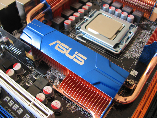
ASUS has managed to create an eye-catching board, from the all-copper cooling solution and the subtle blue tint on the LGA775 socket, to the tasteful expansion slot colors and the black PCB. If appearance is a major factor in your hardware purchases, the P5E3 Premium could be love at first sight; we were certainly impressed by the aesthetic balance. A quick and easy way to distinguish the Premium from the Deluxe (Intel X38 based) variants of the P5E3 series is the deep cobalt blue anodizing on the heatpipe covers and side supports. Although we try not to place too much weight on how a board looks, it's nice that users won't have to compromise with an ugly-but-fast board.
The single-piece heatpipe assembly is entirely capable of controlling Northbridge temperatures, even when pushing the board to its limits. ASUS has improved upon the already impressive mounting system by including screws that do not limit their travel to the point where the heat sink may feel "loose." The portions of the assembly covering the Northbridge and the Southbridge include back plates, a feature that allowed us the ability to ensure optimum heat transfer after we replaced the thermal interface material (TIM) with OCZ Freeze and gave the screws a few extra full turns. The heatsinks located above the power MOSFETs are still attached using plastic pushpins and flimsy metal springs - we would also like to see some black plates for these as hard mounting them would bow the board to the point that some of the components would no longer make proper contact with the heatsinks.
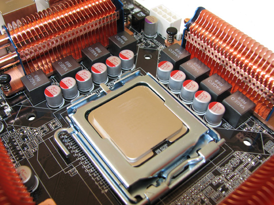
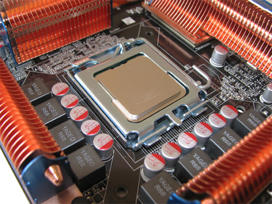
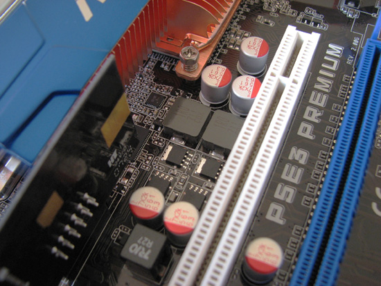
ASUS' power delivery system is among the best in the business at this time. An ADP3228 PWM controller commands an 8-phase solution, made up of low-DCR, solid ferrite-core Yageo inductors, and ultra-low ESR Nichicon capacitors. However, we feel that the two 270uF input power filter capacitors used to remove any ripple in the 12V line coming from the PSU were somewhat undersized for the task. We would like to see capacitors used here which provide at least 2000uF of total supply capacitance. The P5E3 Premium also includes an EPU (Energy Processing Unit), which functions to increase the VRM efficiency 7% by reducing the number of operating phases from eight down to four during periods of light system loading. However, given the incredibly low idle power consumption of Intel 45nm CPUs and G0-step 65nm CPUs, 7% usually works out to rather small savings. Don't expect to see a significant difference in power requirements from this feature alone. Regardless, every bit helps, so we applaud ASUS for their efforts.
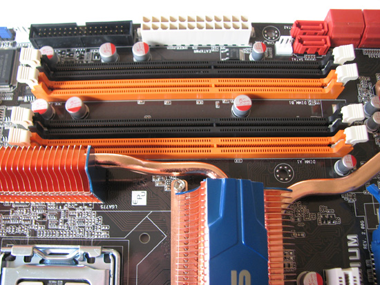
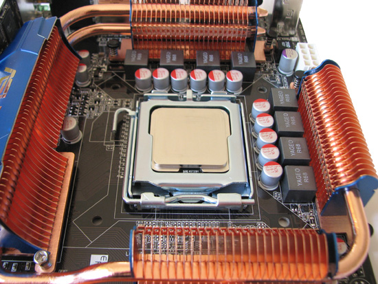
Here we can see the familiar trademark of DDR3 memory expansion slots - no on-board termination resistors. As an aside, one of the many improvements included in the change from DDR2 to DDR3 was the movement of motherboard-level termination resistors to the DIMM modules themselves. A closer look at any DDR3 module should reveal the presence of multiple arrays of 4-pack resistor SMDs used to terminate the command and data signal lines as close to the memory dies as possible. Not only does this improve overall signal integrity, allowing for stable operation at much higher memory speeds, but the memory power delivery solution can benefit as well. Fewer discrete components located near the DDR3 expansion slots means routing of power delivery (VDDQ) and ground planes can be made much cleaner - a fact ASUS takes advantage of by slightly widening the channel spacing to allow for the placement of extra bulk capacitance.
The changes don't end there though. ASUS' new P5E3 Premium is the world's first motherboard to employ a 3-phase memory power solution, shown in the above picture. Out of all the innovations introduced on this motherboard, this was by far one of our favorites. Strong, stable power delivery and solid reference voltages are vital in the success of any memory overclock and this board does not pretend otherwise. Worth noting, we measured the P5E3 Premium as overvolting the memory by about 0.05V with nearly no noticeable droop.
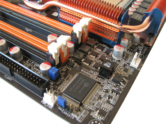
Also seen here are the "OV_CPU" and "OV_NB" jumpers, which select whether or not to allow the use of the higher, secondary voltage ranges available via the BIOS. Most if not all users should find they have no reason to change their positions, as they unlock what we would consider to be ridiculously high voltages. The Winbond SuperIO chip sits at the corner of the board.
Not wanting to be left out, the Northbridge (MCH) is powered by a robust 2-phase system, something we have already grown to expect when it comes to the high-end X48 motherboards. ASUS' implementation is particularly interesting in that their solution utilizes the same exact MOSFETs used in both the CPU and memory power delivery circuits. Again, a clean, stable power supply is vitally important in any overclocking scenario. Our measurements showed the board overvolting the MCH by about 0.05V with about 0.01V of droop under load.


32 Comments
View All Comments
marsbound2024 - Wednesday, February 20, 2008 - link
That is truly the only word I can think of at the moment. While my technical knowledge is above average at best, I can say that I understood plenty enough to know that this is one amazing board. The specifications are really impressive and I was quite happy to see some of the results that you guys were able to coax out of it. I am certainly looking forward to future reviews on the chipset as well as nVidia's upcoming solution.ghd nz - Monday, January 7, 2013 - link
http://www.beats-bydrdre.ca