ASUS ROG Rampage Formula: Why we were wrong about the Intel X48
by Kris Boughton on January 25, 2008 4:30 AM EST- Posted in
- Motherboards
The Basics of Strap Selections, Dividers and Derived Memory Speeds
We have discussed MCH Read Delay (tRD) and its effects on memory read performance before. About a year ago, this particular setting allowed some vendors to design boards that seemed to outperform competing companies' products consistently on a clock-for-clock basis. This was around the time that the enthusiast community first realized the importance of "straps". Some found that by setting a lower strap while running an equivalent Front Side Bus (FSB) that they were able to achieve better performance, higher frame rates, and better benchmark completion times all without the help of any additional tuning.
For those that are unfamiliar with what we mean by strap, consider the following example. Suppose you have two different CPUs, each with a different default FSB, as is the case with first-generation Core 2 processors (266MHz) and current 45nm Core 2 processors (333MHz). If you were to install these processors in identical systems each would be capable of running the same memory speeds (at least DDR2-667 and DDR2-800), regardless of the processor's default FSB. For the 266MHz default FSB processor, this would require a 5:4 and 3:2 divider respectively, while the 333MHz FSB variant would need 1:1 and 6:5. These ratios are necessary in order for the motherboard to set up allowable memory subsystem to system data bus interface configurations.
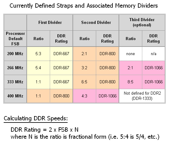
Because of this, the motherboard does not need to know anything about the installed processor and memory, other than the default FSB and the memory's SPD rating, which are both read programmatically prior to Power On Self Test (POST). For example, a 266 FSB processor paired with DDR2-800 memory will make use of the associated 266 strap's second divider - as would a 333 FSB processor. Would you be surprised to learn this works exactly the same way for a 200 FSB processor? Well, it does, and in fact it does not matter which processor type is installed - all combinations work and allow for the same exact memory speeds - DDR2-667 and DDR2-800 (and sometimes DDR2-1066).
If slower memory is detected the system simply uses the first divider in order to achieve DDR2-667 speeds. In the case of faster memory, the third divider is used for DDR2-1066 - which is sometimes available, depending on the strap in use. (All 266, 333, and the upcoming 400 MHz FSB parts will be able to make use of this new official memory speed, as recently announced by JEDEC.) One final note, "down" dividers are no longer possible with Intel platforms and as such the lowest supported memory speed for systems that will make use of the QX9770 (when it arrives) will be DDR2-800, unless the user chooses to underclock the FSB.
As we can see, this system allows for maximum component interchangeability and configuration flexibility all through the use of relatively straightforward selection logic. Check the table below for more information on how to derive these numbers.
Now that we know a little more about what straps are and how they work, we are ready to discuss what they mean when overclocking. Let's say you have an E6700 that makes use of a default FSB of 266MHz - pushing the FSB to 400 while making use of the processor's default strap's second divider (3:2) results in a final memory speed of DDR2-1200, a goal that might be outside the realm of normal achievement unless you have memory capable of this speed. By selecting the 400 strap the 1:1 and 4:3 dividers become available and we are able to set a more modest speed of either DDR2-800 or even DDR2-1066. Alternatively, choosing the 266 strap permits use of the 5:4 divider for DDR2-1000.
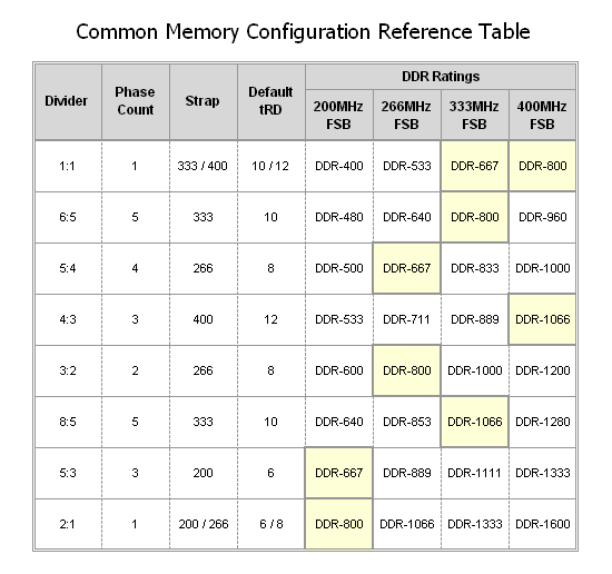
The point is that the freedom to choose any strap we want, regardless of CPU type installed, gives us the choice to make use of a whole myriad of memory speed settings that would otherwise be unavailable. Take note of the "Default tRD" column; you will see that each strap has an associated value (6 at the 200 strap, 8 for 266, etc.) We will discuss this particular setting in detail a little later.
Until now, choosing a memory divider in order to set a final memory speed was easy. Most users focus solely on achieving maximum CPU frequency, letting the memory speed fall where it will. Although it is possible for memory to be the limiting component when overclocking, this is unlikely considering the low cost and high availability of today's performance DDR2 modules. Thus it's easy to pick a memory divider that places the memory operating point near a maximum without ever considering what could be done in order to further improve performance.
Perhaps too many users feel the time they need to invest in fine-tuning their memory settings is not worth the effort. While this might not be far from the truth, we find this hard to believe. Major memory manufactures like OCZ, Corsair, Cell Shock, G.Skill, and Team Group have entire departments of support personnel that work hard every day to provide users the assistance they need to make the most of their purchase. These groups are inundated with requests for help, from both experienced users and novices alike.
Going back to what we said before, what does all of this have to do with better performance on a clock-for-clock basis? In a word: everything! We would like to provide some solid information on the subject as to why the age-old quest for maximum FSB is not always the best approach; in fact, it is often the wrong approach. Our hope is that once allowed an opportunity to make use of this information, users will begin to understand the true limitations of their system components better and might perhaps stop inappropriately blaming overclocking failures on perfectly good hardware. Better yet, they'll stop buying boards based solely on FSB capability when overall system performance is much more important.
Now that we have had a chance to review the basics on memory straps let's move on to something a little more interesting - MCH clock crossing operation and the associated MCH Read Delay (tRD).


73 Comments
View All Comments
Orthogonal - Friday, January 25, 2008 - link
Just so I understand this correctly, due to the path the data and clocks must travel throughout the devices as explained on page 5, even though you can increase the bandwidth of the Memory modules, the MCH is ultimately the "bottleneck". Historically we falsely assumed higher bandwidth and lower CAS latency translated to better data throughput, but since tRD increased along with it, it was essentially wiped out or unused bandwidth. Now we try to lower tRD as low as possible to reduce MCH latency as it performs the "Clock crossing procedure", which is why the 400Mhz FSB with the lowest tRD latency gives the best data throughput.Also, does this mean that in your "Best Pick" DDR2 configuration summary that the two A+ choices highlighted in Green will effectively result in about the same performance since even though DDR2-1200 has more bandwidth than DDR2-1000, since the tRD=5, they will have the same Trd Delay (12.5ns).
Aivas47a - Friday, January 25, 2008 - link
I'm glad to see Asus implementing these new memory phase adjustment options in the bios. Now if they would provide a greater ability to fine-tune GTL reference voltages I would be a happy camper. GTL is a key setting for quad core overclocking success as Raja has helpfully explained in his DFI P35 review. The selectable percentages Asus currently provides are too crude and don't go high enough.mrlobber - Friday, January 25, 2008 - link
FCG, your article just flat out rocks, thanks for this one, we needed it badly :)One question about the previous Asus boards: X38 and also P35, which lack the exact tRD manipulation, providing the Transaction Booster stuff instead. As far as I understand, your analysis about the default tRD values set by different default fsb and memory divider combinations could also be used to determine the starting tRD value at least for the X38 chipset as well in a pretty straightforward way, and from that point being able to offset the tRD with Transaction Booster up or down to control it as necessary? (P35 would have different default tRD's, but the underlying principles should stay the same?)
And, by making appropriate changes in x values if needed, your POST / no POST inequality should stay applicable as well, right?
kjboughton - Friday, January 25, 2008 - link
All true, although we did talk about how these straps at one time had default tRD values associated with them, the difference has become that these default values are now usually based on the real underlying requirements, such as FSB. Now, exactly how each motherboard vendor sets up and implements this value has a lot to do with how their motherboard falls out in comparison testing. With that being said, boards that perform better generally make use of lower tRD values by default. And because X48 is a speed-binned version of X38, which is superior to P35 with it comes to MCH overclocking, it is also safe to say that the higher-end chipsets will allower the same (or lower) tRD values at FSB levels where the other chipsets may fall flat on their faces. Make sense?Regarding the 'Test POST Equation' - absolutely, I know those equations to be true for X38/X48 but I wouldn't doubt if they ended up being exactly the same for say, P35. A little bit of testing should validate this assumption... ;)
Orthogonal - Friday, January 25, 2008 - link
Can we expect a similar analysis and optimization of strappings, timings etc... when an X48 DDR3 compatible board is released?kjboughton - Friday, January 25, 2008 - link
Yes, the will be an easy bridge to make. DDR3 is very similar to DDR2 and in a lot of respects is a simply extension of the logic already developed. In any case, we will provide this information for reference when the time comes.daddyo323 - Friday, January 25, 2008 - link
I've overclocked a couple cpus before, and each time, I had stability problems due to memory.I have built many systems, but since gave up on overclocking... these new Cores and chipsets look like they were made for it...
My question is, was that CPU stable at 4ghz, and could we have a chart on which settings to set, exactly... I wonder how far we can push this platform with the air cooling.
kjboughton - Friday, January 25, 2008 - link
Everything you want to know, about more, about this CPU can be seen here: http://www.anandtech.com/cpuchipsets/intel/showdoc...">http://www.anandtech.com/cpuchipsets/intel/showdoc...We used the same CPU that can be read about in the above review. The short answer is yes, we were completely stable at 4GHz with just 1.28V real under load.
Cheers,
Kris
Quiksilver - Friday, January 25, 2008 - link
Has there been an ETA on the release date of the X48 chipset? I thought they were supposed to come out in December but they never appeared and this would be the second X48 preview I've seen for AT. Also I remember seeing a flow chart somewhere that had DDR2 & DDR3 being the differences between X38 and X48 of which X38 had both but now it seems X48 has DDR2 as well but will the DDR2 boards be available at launch or are they coming later on?Gary Key - Friday, January 25, 2008 - link
ASUS is telling us mid-February for the X48 launch now. Gigabyte and MSI have confirmed that also, but we have had dates confirmed about a dozen times over the last two months and it always seems to change about three days before the next "official" launch. ;)