ASUS ROG Rampage Formula: Why we were wrong about the Intel X48
by Kris Boughton on January 25, 2008 4:30 AM EST- Posted in
- Motherboards
Board Layout, Features and Specifications
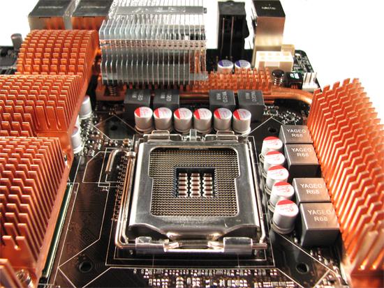
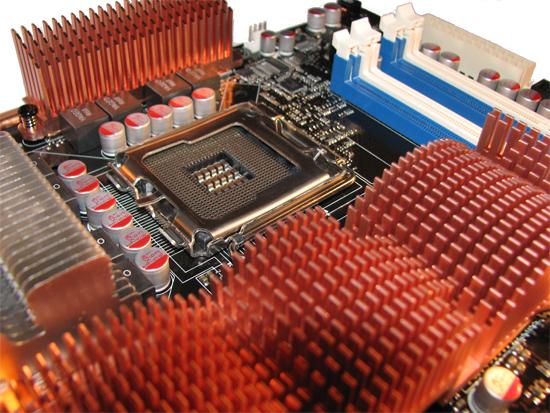
The ASUS Rampage Formula makes use of a beefy 8-phase PWM solution. The copper heatsink covering the MOSFETS is actually not thermally coupled to the Northbridge or the Southbridge as the cooling solution consists of two separate blocks. The hold-down mechanism for the X48's high quality heatsink is comprised of four tension screws attached to a backplate on the opposite side of the board. Besides changing the thermal paste ASUS utilized, we feel there is nothing that needs modification by the end user as long as overclocking aspirations are within reason.
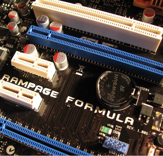
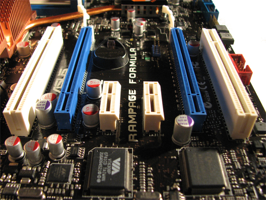
Two full x16 PCI-E 2.0 slots are available for official CrossFire support and the spacing is appropriate. We would have liked an additional PCI slot, for a total of three, instead of the three x1 PCI-E 1.x slots.
Six onboard SATA headers are on the right side of the board, each at 90 degree angles. This made inserting and removing cables easy, even with two full-length video cards installed.
One feature we particularly like is the volt-minder LEDs - one each for the CPU, Northbridge, Southbridge, and memory slots. Each can be one of three colors - green, yellow, or red - and they are useful for determining at a glance the approximate voltage being fed to each component. Green represents "safe" voltages, yellow is elevated (high), and red means "crazy high." Crazy high is just that too, as the board won't set the light red for the CPU voltage until it eclipses about 2.025V.
| ASUS R.O.G. Rampage Formula | |
| Market Segment | Gamer / Extreme Performance - $299.99 (estimated) |
| CPU Interface | Socket T (LGA-775) |
| CPU Support | LGA775-based Core2 Duo, Core2 Extreme, or Core2 Quad recommended, including next-generation 45nm compatibility (06/05B/05A processors) |
| Chipset | Intel X48 Northbridge (MCH) and ICH9R Southbridge |
| CPU Clock Multiplier | 6x ~ 11x, downward adjustable for Core2, upward to 31x for Extreme, half-multiplier support for 45nm processors |
| Front Side Bus Speeds | Auto, 200 ~ 800 in 1MHz increments |
| System Bus Speeds | 1600/1333/1066/800 (MHz) with Official DDR-1066 Support |
| DDR2 Memory Dividers | 1:1, 6:5, 5:4, 4:3, 3:2, 8:5, 5:3, and 2:1 (dependent upon strap setting) |
| FSB Strap | Auto, 200, 266, 333, 400 |
| PCIe Speeds | Auto, 100MHz ~ 180MHz |
| PCI Speeds | Locked at 33.33MHz |
| DRAM Voltage | Auto, 1.80V ~ 3.40V in 0.02V increments, 1.80V standard |
| DRAM CLK/CMD Skew CA/CB | Auto, Manual (Advance/Delay 50ps ~ 350ps in 50ps increments) |
| DRAM Timing Control | Auto, Manual - 20 DRAM Timing Options (tCL, tRCD, tRP, tRAS, tRFC + 15 sub-timings) |
| DRAM Command Rate | Auto, 1N, 2N |
| DRAM Static Read Control | Auto, Enabled, Disabled |
| Ai Clock Twister | Auto, Light, Moderate, Strong |
| Ai Transaction Booster | Auto, Manual |
| Common Performance Level | 1 ~ 31 (settings above 14 prevent POST) |
| CH A/B Phase Pull-In | Based on Memory Divider, All Phases Adjustable (Enabled/Disabled) |
| Core Voltage | Auto, 1.10000 to 1.60000 in 0.00625V increments then 0.05V increments |
| CPU PLL Voltage | Auto, 1.50 ~ 3.00v in 0.02V increments, 1.50V standard |
| FSB Termination Voltage | Auto, 1.20V to 2.00V in 0.02V increments, 1.20V standard |
| North Bridge Voltage | Auto, 1.25V ~ 1.85V in 0.02V increments, 1.25v standard |
| South Bridge Voltage | Auto, 1.050V ~ 1.225V in 0.025V increments, 1.050V standard |
| SB 1.5V Voltage | Auto, 1.50V ~ 2.05V in 0.05V increments, 1.50V standard |
| Loadline Calibration | Auto, Enabled, Disabled |
| CPU Voltage Reference | Auto, x0.63, x0.61, x0.59, x0.57 |
| NB Voltage Reference | Auto, x0.67, x0.63, x0.60, x0.57, x0.56, x0.53, x0.51, x0.49 |
| Memory Slots | Four 240-pin DDR2 DIMM Slots Dual-Channel Configuration Regular Unbuffered, non-ECC DDR2 Memory to 8GB Total |
| Expansion Slots | 2 - PCIe 2.0 x16, Supports ATI CrossFire
Technology 3 - PCIe (1.x) x1, (1) is Compatible with Add-in Audio Card 2 - PCI Slot 2.2 |
| Onboard SATA RAID | 6 SATA 3Gbps Ports - ICH9R (RAID 0, 1, 5, 10) |
| Onboard IDE (PATA) | JMicron JMB368 PATA Controller (up to two UDMA 133/100/66 devices) |
| Onboard USB 2.0/IEEE-1394 | 12 USB 2.0 Ports - (6) I/O Panel - (6) via
Headers 2 IEEE-1394(a) Ports - (1) I/O Panel, (1) via Header |
| Onboard LAN (with Teaming) | Realtek RTL8110SC - PCI Gigabit Ethernet
controller Marvell 88E8056 PCI Express Gigabit Ethernet controller |
| Onboard Audio | ADI 1988B - 8-channel HD Audio CODEC |
| Power Connectors | ATX 24-pin, 8-pin ATX 12V |
| I/O Panel | 1 x PS/2 Keyboard 2 x SPDIF - (1) Optical Out, (1) Coaxial Out 1 x IEEE-1394a 2 x RJ-45 (LAN) 6 x USB 2.0/1.1 1 Clear CMOS Switch |
| Fan Headers | 8 - (1) CPU, (1) Power, (3) Chassis, (3) Optional/Misc. |
| Fan Control | CPU and Chassis Fan Control via BIOS/Extreme Tweaker, PC Probe II monitoring |
| BIOS Revision | v0108 |
| Board Revision | 1.03G |
The ASUS Rampage Formula provides an impressive range of setting specifications. We would go so far as to say that more than a few of these are simply ridiculously high; however, there are sure to be a few people that require these options. A couple of the higher settings to pay attention to: CPU voltage well above 2.0V, CPU PLL voltage to 3.0V (sure to kill your chip super quick), FSB Termination voltage to around 2.0V, and DRAM voltages over 3.4V. While we certainly must commend ASUS on their fine range of control we also feel the need to strongly caution users when working with some of these settings. It's entirely possible to damage or destroy your chipset, CPU, or memory when moving to the extreme limits of these ranges; sometimes less is more.
As we have discussed before Loadline Calibration is best left disabled, especially when using the newer 45nm CPUs. Our testing has shown these settings induce power instabilities, even when using lower voltages. In addition, when enabled the option sometimes requires more CPU voltage than would otherwise be necessary, meaning increased power dissipation and higher temperatures.
Of note, the Rampage Formula allows for half-multiplier usage. This is particularly useful when working in the higher FSB ranges. Because all Core 2 Duo/Quad CPUs are downward unlocked, every half multiplier between the processor default value and 6 can be used, with the exception of 6.5x. For the Extreme processors, this limitation has been relaxed allowing for multipliers as high as 31x in half steps. Besides providing finer CPU frequency control, half-multipliers permit a wider choice of final multiplier/FSB combinations, which can help when choosing the best operating point for the processor and memory. Now that we have experienced what these new values have to offer, it will be hard to work with anything else.
As we pointed out before, "Ai Transaction Booster" is completely revamped for this board series. Setting this option to manual allows the user to take full control of the "Common Performance Level", meaning that all memory phases will baseline at the value as set. Each individual phase can then be "pulled-in" or left as is. "Pulling-in" a phase reduces just that phase's associated tRD value (performance level) by one. Like memory timings, lower values are tighter and thus provide better memory read performance and lower latencies. If all phases are pulled-in, this is the equivalent of selecting the next lower common performance level and performs identically to this new setting. Thus, pulling-in particular phases can allow the user to affect a minor performance improvement if selecting the next lower common performance level is not possible.


73 Comments
View All Comments
Orthogonal - Friday, January 25, 2008 - link
Just so I understand this correctly, due to the path the data and clocks must travel throughout the devices as explained on page 5, even though you can increase the bandwidth of the Memory modules, the MCH is ultimately the "bottleneck". Historically we falsely assumed higher bandwidth and lower CAS latency translated to better data throughput, but since tRD increased along with it, it was essentially wiped out or unused bandwidth. Now we try to lower tRD as low as possible to reduce MCH latency as it performs the "Clock crossing procedure", which is why the 400Mhz FSB with the lowest tRD latency gives the best data throughput.Also, does this mean that in your "Best Pick" DDR2 configuration summary that the two A+ choices highlighted in Green will effectively result in about the same performance since even though DDR2-1200 has more bandwidth than DDR2-1000, since the tRD=5, they will have the same Trd Delay (12.5ns).
Aivas47a - Friday, January 25, 2008 - link
I'm glad to see Asus implementing these new memory phase adjustment options in the bios. Now if they would provide a greater ability to fine-tune GTL reference voltages I would be a happy camper. GTL is a key setting for quad core overclocking success as Raja has helpfully explained in his DFI P35 review. The selectable percentages Asus currently provides are too crude and don't go high enough.mrlobber - Friday, January 25, 2008 - link
FCG, your article just flat out rocks, thanks for this one, we needed it badly :)One question about the previous Asus boards: X38 and also P35, which lack the exact tRD manipulation, providing the Transaction Booster stuff instead. As far as I understand, your analysis about the default tRD values set by different default fsb and memory divider combinations could also be used to determine the starting tRD value at least for the X38 chipset as well in a pretty straightforward way, and from that point being able to offset the tRD with Transaction Booster up or down to control it as necessary? (P35 would have different default tRD's, but the underlying principles should stay the same?)
And, by making appropriate changes in x values if needed, your POST / no POST inequality should stay applicable as well, right?
kjboughton - Friday, January 25, 2008 - link
All true, although we did talk about how these straps at one time had default tRD values associated with them, the difference has become that these default values are now usually based on the real underlying requirements, such as FSB. Now, exactly how each motherboard vendor sets up and implements this value has a lot to do with how their motherboard falls out in comparison testing. With that being said, boards that perform better generally make use of lower tRD values by default. And because X48 is a speed-binned version of X38, which is superior to P35 with it comes to MCH overclocking, it is also safe to say that the higher-end chipsets will allower the same (or lower) tRD values at FSB levels where the other chipsets may fall flat on their faces. Make sense?Regarding the 'Test POST Equation' - absolutely, I know those equations to be true for X38/X48 but I wouldn't doubt if they ended up being exactly the same for say, P35. A little bit of testing should validate this assumption... ;)
Orthogonal - Friday, January 25, 2008 - link
Can we expect a similar analysis and optimization of strappings, timings etc... when an X48 DDR3 compatible board is released?kjboughton - Friday, January 25, 2008 - link
Yes, the will be an easy bridge to make. DDR3 is very similar to DDR2 and in a lot of respects is a simply extension of the logic already developed. In any case, we will provide this information for reference when the time comes.daddyo323 - Friday, January 25, 2008 - link
I've overclocked a couple cpus before, and each time, I had stability problems due to memory.I have built many systems, but since gave up on overclocking... these new Cores and chipsets look like they were made for it...
My question is, was that CPU stable at 4ghz, and could we have a chart on which settings to set, exactly... I wonder how far we can push this platform with the air cooling.
kjboughton - Friday, January 25, 2008 - link
Everything you want to know, about more, about this CPU can be seen here: http://www.anandtech.com/cpuchipsets/intel/showdoc...">http://www.anandtech.com/cpuchipsets/intel/showdoc...We used the same CPU that can be read about in the above review. The short answer is yes, we were completely stable at 4GHz with just 1.28V real under load.
Cheers,
Kris
Quiksilver - Friday, January 25, 2008 - link
Has there been an ETA on the release date of the X48 chipset? I thought they were supposed to come out in December but they never appeared and this would be the second X48 preview I've seen for AT. Also I remember seeing a flow chart somewhere that had DDR2 & DDR3 being the differences between X38 and X48 of which X38 had both but now it seems X48 has DDR2 as well but will the DDR2 boards be available at launch or are they coming later on?Gary Key - Friday, January 25, 2008 - link
ASUS is telling us mid-February for the X48 launch now. Gigabyte and MSI have confirmed that also, but we have had dates confirmed about a dozen times over the last two months and it always seems to change about three days before the next "official" launch. ;)