ASUS ROG Rampage Formula: Why we were wrong about the Intel X48
by Kris Boughton on January 25, 2008 4:30 AM EST- Posted in
- Motherboards
The Basics of Strap Selections, Dividers and Derived Memory Speeds
We have discussed MCH Read Delay (tRD) and its effects on memory read performance before. About a year ago, this particular setting allowed some vendors to design boards that seemed to outperform competing companies' products consistently on a clock-for-clock basis. This was around the time that the enthusiast community first realized the importance of "straps". Some found that by setting a lower strap while running an equivalent Front Side Bus (FSB) that they were able to achieve better performance, higher frame rates, and better benchmark completion times all without the help of any additional tuning.
For those that are unfamiliar with what we mean by strap, consider the following example. Suppose you have two different CPUs, each with a different default FSB, as is the case with first-generation Core 2 processors (266MHz) and current 45nm Core 2 processors (333MHz). If you were to install these processors in identical systems each would be capable of running the same memory speeds (at least DDR2-667 and DDR2-800), regardless of the processor's default FSB. For the 266MHz default FSB processor, this would require a 5:4 and 3:2 divider respectively, while the 333MHz FSB variant would need 1:1 and 6:5. These ratios are necessary in order for the motherboard to set up allowable memory subsystem to system data bus interface configurations.
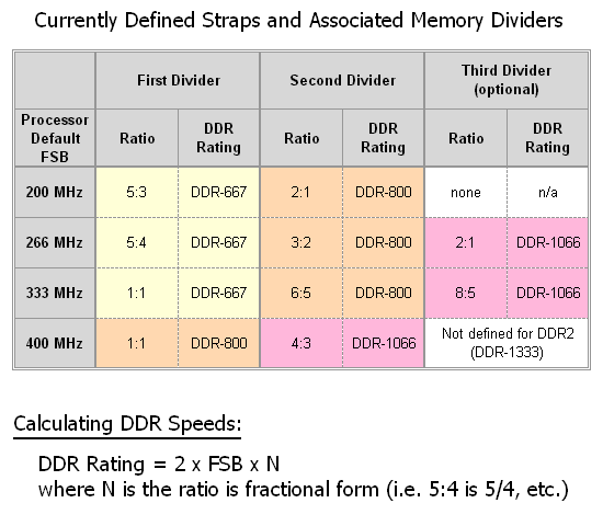
Because of this, the motherboard does not need to know anything about the installed processor and memory, other than the default FSB and the memory's SPD rating, which are both read programmatically prior to Power On Self Test (POST). For example, a 266 FSB processor paired with DDR2-800 memory will make use of the associated 266 strap's second divider - as would a 333 FSB processor. Would you be surprised to learn this works exactly the same way for a 200 FSB processor? Well, it does, and in fact it does not matter which processor type is installed - all combinations work and allow for the same exact memory speeds - DDR2-667 and DDR2-800 (and sometimes DDR2-1066).
If slower memory is detected the system simply uses the first divider in order to achieve DDR2-667 speeds. In the case of faster memory, the third divider is used for DDR2-1066 - which is sometimes available, depending on the strap in use. (All 266, 333, and the upcoming 400 MHz FSB parts will be able to make use of this new official memory speed, as recently announced by JEDEC.) One final note, "down" dividers are no longer possible with Intel platforms and as such the lowest supported memory speed for systems that will make use of the QX9770 (when it arrives) will be DDR2-800, unless the user chooses to underclock the FSB.
As we can see, this system allows for maximum component interchangeability and configuration flexibility all through the use of relatively straightforward selection logic. Check the table below for more information on how to derive these numbers.
Now that we know a little more about what straps are and how they work, we are ready to discuss what they mean when overclocking. Let's say you have an E6700 that makes use of a default FSB of 266MHz - pushing the FSB to 400 while making use of the processor's default strap's second divider (3:2) results in a final memory speed of DDR2-1200, a goal that might be outside the realm of normal achievement unless you have memory capable of this speed. By selecting the 400 strap the 1:1 and 4:3 dividers become available and we are able to set a more modest speed of either DDR2-800 or even DDR2-1066. Alternatively, choosing the 266 strap permits use of the 5:4 divider for DDR2-1000.
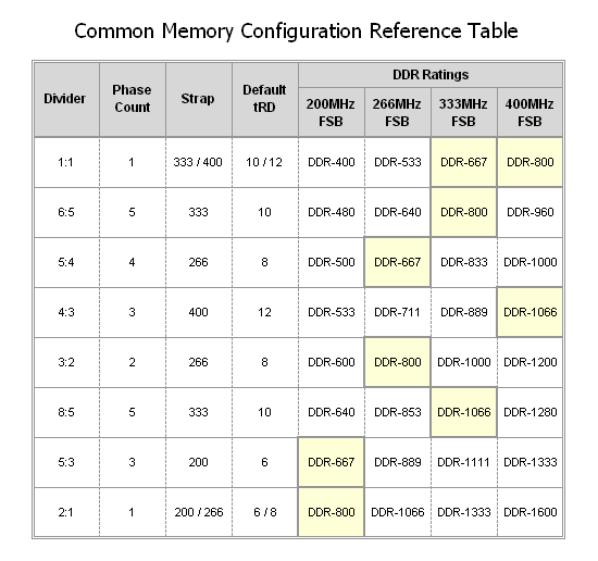
The point is that the freedom to choose any strap we want, regardless of CPU type installed, gives us the choice to make use of a whole myriad of memory speed settings that would otherwise be unavailable. Take note of the "Default tRD" column; you will see that each strap has an associated value (6 at the 200 strap, 8 for 266, etc.) We will discuss this particular setting in detail a little later.
Until now, choosing a memory divider in order to set a final memory speed was easy. Most users focus solely on achieving maximum CPU frequency, letting the memory speed fall where it will. Although it is possible for memory to be the limiting component when overclocking, this is unlikely considering the low cost and high availability of today's performance DDR2 modules. Thus it's easy to pick a memory divider that places the memory operating point near a maximum without ever considering what could be done in order to further improve performance.
Perhaps too many users feel the time they need to invest in fine-tuning their memory settings is not worth the effort. While this might not be far from the truth, we find this hard to believe. Major memory manufactures like OCZ, Corsair, Cell Shock, G.Skill, and Team Group have entire departments of support personnel that work hard every day to provide users the assistance they need to make the most of their purchase. These groups are inundated with requests for help, from both experienced users and novices alike.
Going back to what we said before, what does all of this have to do with better performance on a clock-for-clock basis? In a word: everything! We would like to provide some solid information on the subject as to why the age-old quest for maximum FSB is not always the best approach; in fact, it is often the wrong approach. Our hope is that once allowed an opportunity to make use of this information, users will begin to understand the true limitations of their system components better and might perhaps stop inappropriately blaming overclocking failures on perfectly good hardware. Better yet, they'll stop buying boards based solely on FSB capability when overall system performance is much more important.
Now that we have had a chance to review the basics on memory straps let's move on to something a little more interesting - MCH clock crossing operation and the associated MCH Read Delay (tRD).


73 Comments
View All Comments
Vikendios - Thursday, January 31, 2008 - link
Very Interesting. But I believe that AT is also guilty of perpetuating the chipset/multiple GPU incompatibility (or non-optimization) myths, by not giving us systematic reviews of X38/48 and 680/790i using both ATI and Nvidia twinned cards.And if some BIOS adjustments or driver updates are becessary to twin Nvidia cards under Intel chipsets, or ATI/AMD cards under Nvidia's, kindly tell and guide us.
I'm not a conspiration theorist, but I think there is more than meets the eye in the present situation.
The apparent paradox of Intel (chipsets) pushing AMD (Crossfire) solutions is just marketing cycle hysteresis from the days when ATI was still an independent canadian company.
But both Intel and AMD resent video card chip manufacturers forcing their way into hard-wired motherboard real estate thru the multiple GPU concept, with attendant slot and chipset modifications. With the demise of Via, Intel and AMD believe they can own the chipsets, as long as the motherboard manufacturers are only assemblers.
For Nvidia, multiple GPU is an easy way to extend the life of a good graphic chip until the next generation comes up, but mostly it provides for a temporary proprietary claim on the motherboard design. 3dfx first tried that years ago in Voodoo days and it worked. It worked again when ATI couldn't follow up fast enough on SLI and had to fall in AMD's arms.
Nvidia gambled that SLI would allow it to impose its own chipset business, either by technical or marketing (SLI endorsment) means. What next ? Special gaming CPU's ? That's a dangerous taunt, although Intel doesn't yet dare buy them, or compete directly with them with their own GPU's, out of anti-trust concerns in Brussels.
Holly - Wednesday, January 30, 2008 - link
Excelent description of memory timing magic. Thumbs up :-)FSBastrd - Tuesday, January 29, 2008 - link
I may have come off a little brash with my first comment. The article is pretty sweet, and I was able to read through it without the pictures, but that doesn't mean I wouldn't like to view them. It's not just this article either. Pictures pretty much never load on this website for me.kjboughton - Wednesday, January 30, 2008 - link
Do you run some type of ad blocker? It may be causing problems by incorrectly blocking images from our servers...FSBastrd - Wednesday, January 30, 2008 - link
I'm basically running a stock version of Firefox, so no. Ironically, the ads are just about the only pictures that do load for me. Also, all of the picture for the AnandTech homepage load for me, it's just the pics in the articles This is the only website that really gives me problems. One last thing, some (rare) pictures do load for me from the articles. All in all, it's quite strange, and I can't figure it out.FSBastrd - Tuesday, January 29, 2008 - link
Am I the only one who can't get pictures to load from this site. It would sure make this article a whole lot easier to follow along.sje123 - Tuesday, January 29, 2008 - link
Excellent review as ever!Quick question with regard to Watercooling blocks for this board. It looks more or less identical to the X38 apart from the different chip in the NB, therefore I'm wondering if you could tell me whether or not you think an ASUS X38 NB block would also fit the ASUS X48 Rampage?
is the NB under the cooler the same size etc and are the mouting screws in the same position as the X38 eg the Maximus?
THe SB and the mofset coolers will be the same as the Maximus.
snarfbot - Sunday, January 27, 2008 - link
alright, pretty exciting results here.at trd of 8 (default) at 400mhz 1:1 cas 4, i got 7687mb/s read, and 64ns latency in everest.
at trd of 6 at the same speed, divider and cas setting i got 8089mb/s read, and 59.8ns latency.
then just for fun i bumped the speed upto 500 and loosened the timings to cas 5, at 5:4, i left the trd at 6. at these settings i got 8640mb/s read, and 57.5 latency.
the latency suprised me, as the trd remained the same, and i actually loosened the cas latency.
anyways pretty good results.
processor is a e2140@3200mhz.
snarfbot - Sunday, January 27, 2008 - link
alright, i have a ga-p35-ds3l. im running the fsb at 400, memory at 1:1 cas 4.i set trd to 6 in the bios. based on the formula, it shouldnt even post.
trd(6) - tcl(4)/n(1) =fsb400(2)/1
2=2
im gonna run through sandra and see what the difference is, if there is any, or perhaps this setting doesnt work correctly on this board.
Fyl - Sunday, January 27, 2008 - link
not to lower the merits of this great article but since I've read it I've been experimenting on my machine different settings and for some of them your formula doesn't seem to stand; here's an example of a stable configuration, no overvoltage to anything:E8500@3.6 (400MHzx9)
P35-DS4 (tRD 7)
2x2G DDR2 800 (400MHz, 5-5-5-12)
based on your formula N = 400:400 = 1 and x = 2
therefore 7-(5/1) > 2/1 => 2 > 2 => false but actually working
am I missing anything?