ASUS ROG Rampage Formula: Why we were wrong about the Intel X48
by Kris Boughton on January 25, 2008 4:30 AM EST- Posted in
- Motherboards
Board Layout, Features and Specifications
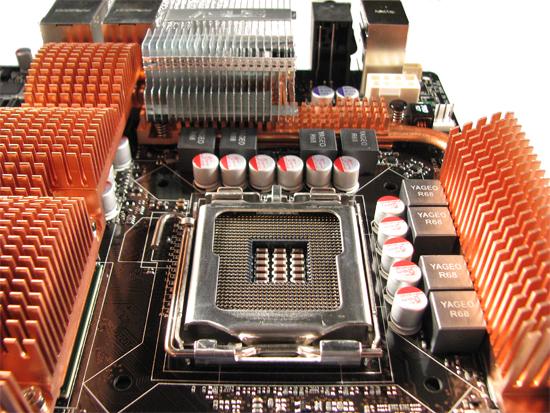
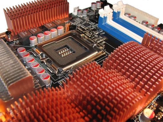
The ASUS Rampage Formula makes use of a beefy 8-phase PWM solution. The copper heatsink covering the MOSFETS is actually not thermally coupled to the Northbridge or the Southbridge as the cooling solution consists of two separate blocks. The hold-down mechanism for the X48's high quality heatsink is comprised of four tension screws attached to a backplate on the opposite side of the board. Besides changing the thermal paste ASUS utilized, we feel there is nothing that needs modification by the end user as long as overclocking aspirations are within reason.
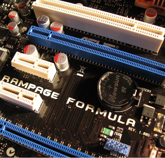
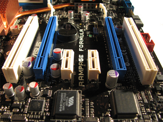
Two full x16 PCI-E 2.0 slots are available for official CrossFire support and the spacing is appropriate. We would have liked an additional PCI slot, for a total of three, instead of the three x1 PCI-E 1.x slots.
Six onboard SATA headers are on the right side of the board, each at 90 degree angles. This made inserting and removing cables easy, even with two full-length video cards installed.
One feature we particularly like is the volt-minder LEDs - one each for the CPU, Northbridge, Southbridge, and memory slots. Each can be one of three colors - green, yellow, or red - and they are useful for determining at a glance the approximate voltage being fed to each component. Green represents "safe" voltages, yellow is elevated (high), and red means "crazy high." Crazy high is just that too, as the board won't set the light red for the CPU voltage until it eclipses about 2.025V.
| ASUS R.O.G. Rampage Formula | |
| Market Segment | Gamer / Extreme Performance - $299.99 (estimated) |
| CPU Interface | Socket T (LGA-775) |
| CPU Support | LGA775-based Core2 Duo, Core2 Extreme, or Core2 Quad recommended, including next-generation 45nm compatibility (06/05B/05A processors) |
| Chipset | Intel X48 Northbridge (MCH) and ICH9R Southbridge |
| CPU Clock Multiplier | 6x ~ 11x, downward adjustable for Core2, upward to 31x for Extreme, half-multiplier support for 45nm processors |
| Front Side Bus Speeds | Auto, 200 ~ 800 in 1MHz increments |
| System Bus Speeds | 1600/1333/1066/800 (MHz) with Official DDR-1066 Support |
| DDR2 Memory Dividers | 1:1, 6:5, 5:4, 4:3, 3:2, 8:5, 5:3, and 2:1 (dependent upon strap setting) |
| FSB Strap | Auto, 200, 266, 333, 400 |
| PCIe Speeds | Auto, 100MHz ~ 180MHz |
| PCI Speeds | Locked at 33.33MHz |
| DRAM Voltage | Auto, 1.80V ~ 3.40V in 0.02V increments, 1.80V standard |
| DRAM CLK/CMD Skew CA/CB | Auto, Manual (Advance/Delay 50ps ~ 350ps in 50ps increments) |
| DRAM Timing Control | Auto, Manual - 20 DRAM Timing Options (tCL, tRCD, tRP, tRAS, tRFC + 15 sub-timings) |
| DRAM Command Rate | Auto, 1N, 2N |
| DRAM Static Read Control | Auto, Enabled, Disabled |
| Ai Clock Twister | Auto, Light, Moderate, Strong |
| Ai Transaction Booster | Auto, Manual |
| Common Performance Level | 1 ~ 31 (settings above 14 prevent POST) |
| CH A/B Phase Pull-In | Based on Memory Divider, All Phases Adjustable (Enabled/Disabled) |
| Core Voltage | Auto, 1.10000 to 1.60000 in 0.00625V increments then 0.05V increments |
| CPU PLL Voltage | Auto, 1.50 ~ 3.00v in 0.02V increments, 1.50V standard |
| FSB Termination Voltage | Auto, 1.20V to 2.00V in 0.02V increments, 1.20V standard |
| North Bridge Voltage | Auto, 1.25V ~ 1.85V in 0.02V increments, 1.25v standard |
| South Bridge Voltage | Auto, 1.050V ~ 1.225V in 0.025V increments, 1.050V standard |
| SB 1.5V Voltage | Auto, 1.50V ~ 2.05V in 0.05V increments, 1.50V standard |
| Loadline Calibration | Auto, Enabled, Disabled |
| CPU Voltage Reference | Auto, x0.63, x0.61, x0.59, x0.57 |
| NB Voltage Reference | Auto, x0.67, x0.63, x0.60, x0.57, x0.56, x0.53, x0.51, x0.49 |
| Memory Slots | Four 240-pin DDR2 DIMM Slots Dual-Channel Configuration Regular Unbuffered, non-ECC DDR2 Memory to 8GB Total |
| Expansion Slots | 2 - PCIe 2.0 x16, Supports ATI CrossFire
Technology 3 - PCIe (1.x) x1, (1) is Compatible with Add-in Audio Card 2 - PCI Slot 2.2 |
| Onboard SATA RAID | 6 SATA 3Gbps Ports - ICH9R (RAID 0, 1, 5, 10) |
| Onboard IDE (PATA) | JMicron JMB368 PATA Controller (up to two UDMA 133/100/66 devices) |
| Onboard USB 2.0/IEEE-1394 | 12 USB 2.0 Ports - (6) I/O Panel - (6) via
Headers 2 IEEE-1394(a) Ports - (1) I/O Panel, (1) via Header |
| Onboard LAN (with Teaming) | Realtek RTL8110SC - PCI Gigabit Ethernet
controller Marvell 88E8056 PCI Express Gigabit Ethernet controller |
| Onboard Audio | ADI 1988B - 8-channel HD Audio CODEC |
| Power Connectors | ATX 24-pin, 8-pin ATX 12V |
| I/O Panel | 1 x PS/2 Keyboard 2 x SPDIF - (1) Optical Out, (1) Coaxial Out 1 x IEEE-1394a 2 x RJ-45 (LAN) 6 x USB 2.0/1.1 1 Clear CMOS Switch |
| Fan Headers | 8 - (1) CPU, (1) Power, (3) Chassis, (3) Optional/Misc. |
| Fan Control | CPU and Chassis Fan Control via BIOS/Extreme Tweaker, PC Probe II monitoring |
| BIOS Revision | v0108 |
| Board Revision | 1.03G |
The ASUS Rampage Formula provides an impressive range of setting specifications. We would go so far as to say that more than a few of these are simply ridiculously high; however, there are sure to be a few people that require these options. A couple of the higher settings to pay attention to: CPU voltage well above 2.0V, CPU PLL voltage to 3.0V (sure to kill your chip super quick), FSB Termination voltage to around 2.0V, and DRAM voltages over 3.4V. While we certainly must commend ASUS on their fine range of control we also feel the need to strongly caution users when working with some of these settings. It's entirely possible to damage or destroy your chipset, CPU, or memory when moving to the extreme limits of these ranges; sometimes less is more.
As we have discussed before Loadline Calibration is best left disabled, especially when using the newer 45nm CPUs. Our testing has shown these settings induce power instabilities, even when using lower voltages. In addition, when enabled the option sometimes requires more CPU voltage than would otherwise be necessary, meaning increased power dissipation and higher temperatures.
Of note, the Rampage Formula allows for half-multiplier usage. This is particularly useful when working in the higher FSB ranges. Because all Core 2 Duo/Quad CPUs are downward unlocked, every half multiplier between the processor default value and 6 can be used, with the exception of 6.5x. For the Extreme processors, this limitation has been relaxed allowing for multipliers as high as 31x in half steps. Besides providing finer CPU frequency control, half-multipliers permit a wider choice of final multiplier/FSB combinations, which can help when choosing the best operating point for the processor and memory. Now that we have experienced what these new values have to offer, it will be hard to work with anything else.
As we pointed out before, "Ai Transaction Booster" is completely revamped for this board series. Setting this option to manual allows the user to take full control of the "Common Performance Level", meaning that all memory phases will baseline at the value as set. Each individual phase can then be "pulled-in" or left as is. "Pulling-in" a phase reduces just that phase's associated tRD value (performance level) by one. Like memory timings, lower values are tighter and thus provide better memory read performance and lower latencies. If all phases are pulled-in, this is the equivalent of selecting the next lower common performance level and performs identically to this new setting. Thus, pulling-in particular phases can allow the user to affect a minor performance improvement if selecting the next lower common performance level is not possible.


73 Comments
View All Comments
Vikendios - Thursday, January 31, 2008 - link
Very Interesting. But I believe that AT is also guilty of perpetuating the chipset/multiple GPU incompatibility (or non-optimization) myths, by not giving us systematic reviews of X38/48 and 680/790i using both ATI and Nvidia twinned cards.And if some BIOS adjustments or driver updates are becessary to twin Nvidia cards under Intel chipsets, or ATI/AMD cards under Nvidia's, kindly tell and guide us.
I'm not a conspiration theorist, but I think there is more than meets the eye in the present situation.
The apparent paradox of Intel (chipsets) pushing AMD (Crossfire) solutions is just marketing cycle hysteresis from the days when ATI was still an independent canadian company.
But both Intel and AMD resent video card chip manufacturers forcing their way into hard-wired motherboard real estate thru the multiple GPU concept, with attendant slot and chipset modifications. With the demise of Via, Intel and AMD believe they can own the chipsets, as long as the motherboard manufacturers are only assemblers.
For Nvidia, multiple GPU is an easy way to extend the life of a good graphic chip until the next generation comes up, but mostly it provides for a temporary proprietary claim on the motherboard design. 3dfx first tried that years ago in Voodoo days and it worked. It worked again when ATI couldn't follow up fast enough on SLI and had to fall in AMD's arms.
Nvidia gambled that SLI would allow it to impose its own chipset business, either by technical or marketing (SLI endorsment) means. What next ? Special gaming CPU's ? That's a dangerous taunt, although Intel doesn't yet dare buy them, or compete directly with them with their own GPU's, out of anti-trust concerns in Brussels.
Holly - Wednesday, January 30, 2008 - link
Excelent description of memory timing magic. Thumbs up :-)FSBastrd - Tuesday, January 29, 2008 - link
I may have come off a little brash with my first comment. The article is pretty sweet, and I was able to read through it without the pictures, but that doesn't mean I wouldn't like to view them. It's not just this article either. Pictures pretty much never load on this website for me.kjboughton - Wednesday, January 30, 2008 - link
Do you run some type of ad blocker? It may be causing problems by incorrectly blocking images from our servers...FSBastrd - Wednesday, January 30, 2008 - link
I'm basically running a stock version of Firefox, so no. Ironically, the ads are just about the only pictures that do load for me. Also, all of the picture for the AnandTech homepage load for me, it's just the pics in the articles This is the only website that really gives me problems. One last thing, some (rare) pictures do load for me from the articles. All in all, it's quite strange, and I can't figure it out.FSBastrd - Tuesday, January 29, 2008 - link
Am I the only one who can't get pictures to load from this site. It would sure make this article a whole lot easier to follow along.sje123 - Tuesday, January 29, 2008 - link
Excellent review as ever!Quick question with regard to Watercooling blocks for this board. It looks more or less identical to the X38 apart from the different chip in the NB, therefore I'm wondering if you could tell me whether or not you think an ASUS X38 NB block would also fit the ASUS X48 Rampage?
is the NB under the cooler the same size etc and are the mouting screws in the same position as the X38 eg the Maximus?
THe SB and the mofset coolers will be the same as the Maximus.
snarfbot - Sunday, January 27, 2008 - link
alright, pretty exciting results here.at trd of 8 (default) at 400mhz 1:1 cas 4, i got 7687mb/s read, and 64ns latency in everest.
at trd of 6 at the same speed, divider and cas setting i got 8089mb/s read, and 59.8ns latency.
then just for fun i bumped the speed upto 500 and loosened the timings to cas 5, at 5:4, i left the trd at 6. at these settings i got 8640mb/s read, and 57.5 latency.
the latency suprised me, as the trd remained the same, and i actually loosened the cas latency.
anyways pretty good results.
processor is a e2140@3200mhz.
snarfbot - Sunday, January 27, 2008 - link
alright, i have a ga-p35-ds3l. im running the fsb at 400, memory at 1:1 cas 4.i set trd to 6 in the bios. based on the formula, it shouldnt even post.
trd(6) - tcl(4)/n(1) =fsb400(2)/1
2=2
im gonna run through sandra and see what the difference is, if there is any, or perhaps this setting doesnt work correctly on this board.
Fyl - Sunday, January 27, 2008 - link
not to lower the merits of this great article but since I've read it I've been experimenting on my machine different settings and for some of them your formula doesn't seem to stand; here's an example of a stable configuration, no overvoltage to anything:E8500@3.6 (400MHzx9)
P35-DS4 (tRD 7)
2x2G DDR2 800 (400MHz, 5-5-5-12)
based on your formula N = 400:400 = 1 and x = 2
therefore 7-(5/1) > 2/1 => 2 > 2 => false but actually working
am I missing anything?