Overclocking Intel's New 45nm QX9650: The Rules Have Changed
by Kris Boughton on December 19, 2007 2:00 AM EST- Posted in
- CPUs
The Origins of Static Read Control Delay (tRD)
With over a year of experience overclocking the Core 2 family of processors, we have learned a thing or two. One of the most important items we've learned is that higher FSB settings do not necessarily mean better performance. Understandably, this may come as a shock to some. For whatever reason, even a lot of well-regarded, seasoned overclockers seem to place great value in achieving the highest possible FSB. Based on what we know, we always establish our base target MCH overclock at the same spot - 400MHz FSB with a tRD of 6. The only other potential base MCH target value even worth considering is 450MHz with a tRD of 7, which should only be used when extra memory speed is needed or when a low maximum CPU multiplier becomes a limiting factor. Without getting into too much detail, let's examine what we mean by this.
When it comes to overclocking, the MCH functions as a hybrid of sorts. Like a CPU, it has an upper frequency limit and more voltage can often raise this limit. On the other hand, since it interfaces with memory it also behaves somewhat like memory with internal "timings" whose absolute values derive from the established FSB.
Consider the case of memory rated to run DDR-800 at CAS 3. We can calculate the absolute CAS (Column Address Strobe) delay in a few quick steps. DDR-800, which is in fact double date rate as the name suggests, runs at a base frequency of 400MHz or 400 million cycles per second. Inverting this value tells us the number of seconds per cycle (2.50ns). Finally, multiplying this by the CAS rating tells us the total delay time of 7.5ns (3 x 2.5ns). Likewise, setting a CAS value of 4 results in an absolute CAS delay of 10ns. We can see now why higher CAS values give way to lower memory bandwidths - in the case described above the MCH spends more time "waiting" for data to become available when the memory is set to CAS 4.
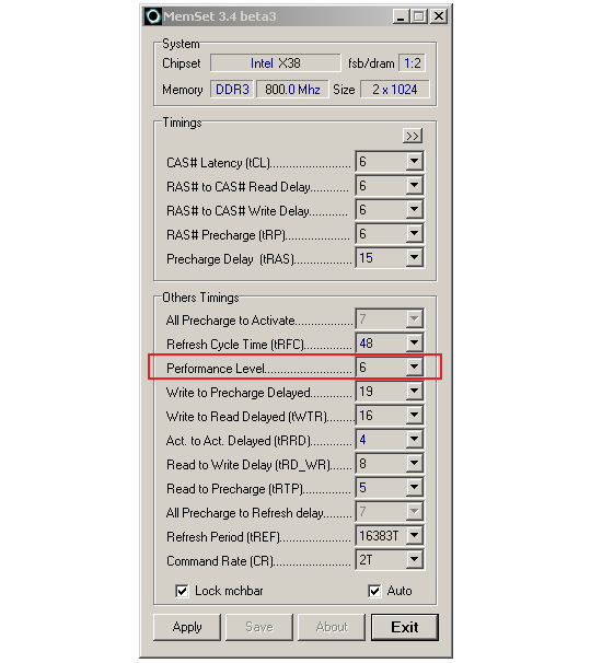
tRD in hiding…we promise we didn't make up the horrible "Performance Level" moniker
Arguably, the most important MCH setting when it comes to performance tweaking is the Static Read Control Delay (tRD) value. Like the memory CAS (CL), setting this value is relative to FSB. Case in point, a tRD value of 6, calculated in the same manner as used before, tells us that MCH sets a read delay of 15ns at an FSB of 400MHz. This means that in addition to the time required for the CPU to issue a request for data in memory to the MCH, the time the MCH spends translating and issuing the command to the memory, and the time the memory requires in retrieving the requested data, the MCH will spend an additional 15ns simply waiting for valid data to become available before fulfilling the CPU's original read request. Obviously, anything that can minimize this wait will be beneficial in improving memory read bandwidth and quite possibly overall system performance.
Until recently, direct tRD manipulation by the user was not even possible. In fact, for the longest time BIOS engineers had no choice but to accept this setting as essentially "hard-coded", making MCH performance rather lackluster. The only way to increase memory subsystem performance was to run at higher FSB settings or tighten primary memory timings. At some point, the MCH design teams got tired of the CPU people hogging all the glory and in a well-calculated effort to boost MCH performance exposed this setting for external programming.
The outside world's first introduction to variable tRD settings came when a few overclockers noticed that setting lower MCH "straps" allowed for higher memory bandwidths. What they didn't know at the time was that they had unintentionally stumbled upon tRD. Tricking the motherboard into detecting an installed CPU as an 800 FSB (200MHz) part forced the MCH into setting a lower tRD value than if the FSB were 1066 (266MHz). Consequently, overclocking the system to the same higher FSB value with the lower strap setting yielded higher memory performance. Often times the effect was significant enough that real-world performance was higher even with a lower final FSB. The tradeoff was apparent however: a lower strap meant a lower maximum FSB. The MCH tRD value, just like a memory timing, must eventually be loosened in order to scale higher. What's more, as is the case with memory, additional voltage can sometimes allow the MCH to run with tighter "timings" at higher speeds.
Eventually the inevitable next step in memory performance tuning became a reality. The option to adjust tRD independent of MCH strap selection became part of every overclocker's arsenal. Nowadays the MCH strap setting does little more than determine which memory multiplier ratios are available for use. Although tRD adjustments are now possible in many BIOS implementations, some motherboard manufactures choose to obfuscate their true nature by giving the setting confusing, proprietary names like "Transaction Booster" and the like. Don't let these names fool you; in the end they all do the same thing: manipulate tRD.


56 Comments
View All Comments
Kougar - Thursday, December 20, 2007 - link
This was the exact type of article I love to sit down and read through. It doesn't matter if portions of it are above my head, it just gets me to rise up another level to grab at them. Your article was a great read and I very much hope to see many more like this one in the future!Regarding the P5E3, I am somewhat surprised that 0.81v was the lowest you could set. Even the budget board P31-DS3L offers 0.51v as an option, my personal P35-DQ6 has 0.50v as a vCore option. I found your commentary regarding Load Line Calibration to be illuminating... this is exactly what enthusiasts like myself and others need to know.
Lastly, I hate to ask here but Google was no help, Intel's ARK database didn't cover it, and Intel's datasheet didn't mention that I could see... what exactly is P35's process size and default vCore? The same as X38's...? As much as I love Gigabyte they are notorious for their lack of system voltage info...
kjboughton - Thursday, December 20, 2007 - link
The P35 and X38 chipsets are both made using Intel's standard 90nm process technology. It's not uncommon for chipset's to lag behind current CPU offerings by a whole process generation or more. With that being said, Intel's upcoming P45 chipset, the last of it's kind (recall that all future CPU technologies will make use of an onboard memory controllers) will be made on the 65nm process -- something even the X48 won't have. In fact, this reduction in process size may have considerable benefits for P45 when it comes to the reduction in power consumption and increased performance headroom, particularlly when overclocking. The P45 default Vmch is 1.15V, X38 is slightly higer at 1.25V. Based on this I would expect to see the P45 come in around 1.05V or possibly even lower.myocardia - Thursday, December 20, 2007 - link
Kris, great article. But, when did $400-500 worth of watercooling equipment become so commonplace, as to be putting the one (or is that two?) companies who make phase-change units out of business? If freon is no longer needed for extreme CPU cooling, couldn't Vapochill just start making even more expensive, higher-end watercooling?spamme33 - Thursday, December 20, 2007 - link
I have been overclocking since my first computer build years and years ago, rarely do I learn that much from one article. Very well written, informative, and timely!kilkennycat - Thursday, December 20, 2007 - link
The documentation accompanying the BIOS settings of almost all enthusiast motherboards is frequently obscure and incomplete - probably because it is printed many months before the board/BIOS is released, plus the leading manufacturers never bother to update BIOS user-documentation when they update the BIOS. Also, it does seem that the documentation authors have a uniformly poor grasp of the English language and prefer to keep descriptions of all BIOS settings as vague and incomprehensible as possible. It is also so common to find sundry BIOS entries not documented AT ALL anywhere in the motherboard manual, even the (so-called) latest on-line version.So I have a request on behalf of those like myself desperately trying to understand each entry in the BIOS of that brand-new and very expensive enthusiastic motherboard that I have just purchased, with that abysmal so-called user-manual and pathetic in-BIOS "Help" Function-key :-
Would it be possible for you or other at Anandtech to fully document/explain all the terms used in the text of the CPU and memory BIOS settings of the most popular enthusiast motherboards?
To keep such an exercise manageable, I suggest confining the exercise initially to existing and upcoming enthusiast desktop motherboards that are fully compatible with Penryn and Phenom. At present, X48, nVidia 780i, AMD 790FX.....
poohbear - Thursday, December 20, 2007 - link
thank you very much for such an informative and detailed article. very much appreciated for us overclockers and the future looks fantabulous w/ these cpus.wyemarn - Thursday, December 20, 2007 - link
Thank you very much for this great article. What a wonderful Christmas gift from Anandtech! This is one the most complete article I have ever read. CPU performance, overclocking, mobo settings, power consumption all in one article. What a joy to read.akaevile - Thursday, December 20, 2007 - link
Thank you for the detailed information. One has to be a little nervous however for the implications in what your work has found. Will Intel's improvements in refining 45nm technology push the line or has it been drawn in the sand??n7 - Wednesday, December 19, 2007 - link
Really superb article.Possibly the best i've ever seen on AT!
Thanx for the indepth info!
Bozo Galora - Wednesday, December 19, 2007 - link
looks like not only the X48, but three 45nm quads also will be delayed - due to AMD incompetence.http://www.digitimes.com/mobos/a20071218PD212.html">http://www.digitimes.com/mobos/a20071218PD212.html