X38 Details
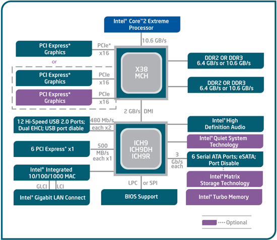
We have the familiar Intel block diagram that basically outlines the same technology patterns in previous MCH/ICH families. The X38 MCH is paired with the ICH9 series of Southbridges that was introduced with the P35 chipset. Intel continues to utilize its Direct Media Interface (DMI) technology for the interconnect link between the ICH/MCH chipsets. The 2GB/s DMI capability has not changed with this latest offering and continues to offer more than enough bandwidth for most users.
We say "most users" as installing a six drive RAID 10 array, audio card, Turbo Memory card, and TV Tuner card along with fully utilizing the LAN and USB ports can provide enough interconnect clogging data that even the most hardened air traffic controller (i.e. chipset) would fly into a panic. However, that particular scenario is very rare on the desktop. Intel will be abandoning the DMI interface late next year when the second generation 45nm CPU, Nehalem, is introduced. Intel's CSI (Common System Interconnect) and IMC (Integrated Memory Controller) represent their long-awaited response to AMD's HyperTransport technology and do away with the current front side bus architecture.
The most significant changes in the X38 MCH over the P35 or 975X are the inclusion of two PCI Express x16 lanes, PCI Express 2.0, and official support for DDR3-1333. One of the features in the X38 MCH that Intel has been fairly quiet about is the revised Snoop feature. It's not what you think, as we can confirm that Snoop Dogg was not involved in this development nor is it a feature that lets NFL head coaches steal signals, or the NSA figure out what you had for breakfast.
While Intel's press slides simply tout the virtues of Intel's "faster memory access", the fact is Intel has revamped the X38's memory controller to include their revised "flexible clock crossing architecture" and improved prefetching circuitry. We have done a little digging into exactly what faster memory access means and it seems to revolve around the snoop cache buffer improvements. The snoop feature can be described very simply as an extra level of pseudo-cache resident in the MCH. It's not really cache, per-se, but lines of recently cached memory reads. The purpose of this feature is to reduce memory read latencies in memory intensive programs that read a lot of data in parallel. The most common scenario is in multiple core computations where the cores are all manipulating shared data a little differently.
The primary benefit is that a separate memory read isn't needed every time data is accessed; instead the X38 MCH intelligently caches data and provides it when available. This also allows for a larger re-order buffer for read and write operations that further enhances memory performance. Every time the MCH must switch between reading and writing there is a wait period on the data lines, so the X38 MCH will wait until there are enough write requests stored before committing the data to memory.
Essentially, the MCH will "store" write requests and then "burst" them into memory when either the filter is full or the core requests data from memory that has not been written yet. So when the MCH writes this data it is coming straight from the pseudo-cache and this is what provides the "faster memory access" in the X38. It is almost like the chipset engineers followed their CPU brethren in the op re-ordering design in the Core 2 series, only it is applied to memory read/writes and implemented by the MCH - or maybe it's just a highly refined feature from the Intel 870. In reality, we have noticed slightly improved latencies and read rates when compared to the P35, but nothing that would make us dance in streets.
Along with support for both DDR2 and DDR3, the X38 introduces official support for DDR3-1333 while the P35 only officially supports DDR3-1066 - even though we have not had any issues running P35 boards past DDR3-2000 with the right memory. Intel is also introducing their Extreme Memory Profile (XMP) technology with the X38 roll-out. XMP is just like the Enhanced Performance Profile (EPP) technology launched by NVIDIA last year. It simply is a means of adding additional memory timing and clock speed profiles to the DDR3 SPDs in the same way EPP does for DDR2 memory. These profiles are designed to make it easier for users to basically auto-tune or overclock their memory/system using specific XMP profiles instead of manually changing individual timings and bus speeds in the BIOS.
Fortunately for those wanting to upgrade to the latest Intel chipset and not needing a new home equity loan to purchase DDR3 modules, the X38 MCH also supports DDR2 memory. In early testing with retail boards and BIOS releases, we are not seeing any real improvements over the DDR2 based P35 boards. Since the X38 is not "optimized" for DDR2 memory operations, this is both good and bad news. However, until DDR3 memory prices subside, an upgrade from the P965 or 975X should not be too painful once boards are in plentiful supply.
The last new feature from Intel is the support for the PCI Express 2.0 standard. In fact, Intel has the first desktop chipset on the market that supports this new standard. (AMD's RD790 should appear in the not-too-distant future.) The big news is the PCI Express 2.0 specification doubles the interconnect bit rate from 2.5 GT/s to 5 GT/s per port and is completely cross-compatible with the 1.0/1.1 specifications.
This means several things. First is that the performance increase to 5 GT/s effectively increases the aggregate bandwidth of a 16-lane link to approximately 16GB/s (maximum theoretical bandwidth of 8GB/s in each direction simultaneously before overhead), double that of the 1.1 spec. Real bandwidth per lane will be up to 4Gb/s (estimated to be around 500MB/s per lane/pin on average in current testing) in each direction given the 8b/10b encoding method used to transmit the data.
This increase in bandwidth comes courtesy of faster signaling rather than wider data paths which is why a 2.0 card is compatible in a 1.01/1.1 slot and vice versa. However, a 1.0/1.1 card will only work at its rated speed in a 2.0 slot and a 2.0 card is limited to the 1.0/1.1 slot speed. When two 16-lane PCI Express ports are utilized, the second port will support PCIe 1.1 cards at x8, x4, or x1 speeds or PCI Express Graphic cards at x16 or x1 operation.
While most will concur the reasoning behind the upgrade to the PCI Express standard is to improve graphics bandwidth, we think several other revised features also played a part in the early adoption of this specification. These features include dynamic link speed management, link bandwidth notification, access control services, and the power limit redefinition protocol. Of these, the dynamic link speed management and power limit redefinition are the two most interesting features in our opinion.
The dynamic link speed feature includes support for software controls that can dynamically throttle lane speeds. The power limit redefinition feature allows the system to redefine the slot power limits based upon the device inserted into that slot. The latter feature will work well with the new 300W electro-mechanical (CEM) spec. This new specification that works on either PCI Express standard provides full support for the 8-pin auxiliary power connectors seen on video cards like the HD 2900 XT and upcoming NVIDIA G9x offerings. The 8-pin PCIe power connector is capable of delivering up to 150W of power compared to the 75W limit in the 6-pin PCIe power plug. The PCI Express x16 slot on the motherboard is still limited to 75W. In total, up to 300W is available for each x16 PCIe slot on the motherboard, and hopefully we will not reach the day where that capability will need to be increased. (The HD 2900XT design had us wondering for awhile....)


14 Comments
View All Comments
Owls - Wednesday, October 10, 2007 - link
The odd thing is why CF is supported but not SLI. I'm guessing nVidia is not giving up this to intel?JarredWalton - Wednesday, October 10, 2007 - link
SLI is an NVIDIA technology, and it is currently limited to only running on NVIDIA chipsets (by the SLI drivers - not by anything else). There are some exceptions - SLI notebooks for example use 945GM chipsets from Intel - but what it basically amounts to is that no one has thrown enough money at NVIDIA to get them to open the standard.Now, there are a few things to consider. First, CrossFire often appears to require additional driver tweaks to run on new chipsets - X38 today, P35 previously, etc. If NVIDIA opened support, we might see additional compatibility problems on other chipsets. That would require more effort from their driver team, presumably, so perhaps they are just trying to keep from overextending.
More likely, however, is that NVIDIA likes being able to push their own chipsets with their graphics hardware. Probably the chipset division doesn't want to become marginalized by opening SLI support to others. This is a bit odd, though, as the profit margins on $300+ graphics cards are much higher (for NVIDIA) than on $100-$200 motherboards. Given how many people have P965 and P35 chipset boards (and even some AMD chipset boards), NVIDIA could probably sell a reasonable number of additional GPUs if they would open up SLI support for these platforms. Who cares about the money from Intel if it means you can gain a bigger advantage over AMD/ATI and still make $100 per GPU sold (or whatever it is they get paid per GPU chipset)?
Well, obviously some higher-ups at NVIDIA care, but I can't help but wonder if they're wearing blinders. Nothing like cutting off your nose to spite your face.
lopri - Thursday, October 11, 2007 - link
Disagreed. SLI has been and will remain the thing for NV in the foreseeable future. I would go as far as to say that one of the biggest factor that drove ATI out of the business is NV's platformization strategy based on SLI and ATI's struggle to catch up.Although the number of people who actually run dual GPUs in tandem might be small, SLI has more meaning to it. (Just like brand-name value or trademarks) Now that Intel is getting ready for high-end discrete GPU market, NV won't give up SLI without a significant return.
8steve8 - Wednesday, October 10, 2007 - link
oh yeah and we are awaiting the triple play of amd products being anounced in november,,, is it still thought that only an extreme version of pheonom will be available in the channel before xmas? or will there be a q6600 class product from amd before xmas?