EVGA 680i LT SLI: NVIDIA's 680i Cost Reduced
by Gary Key on March 28, 2007 4:00 AM EST- Posted in
- CPUs
Since our first look at the 680i SLI chipset back in November we have been impressed with its performance and overall features. What was even more impressive was the fact that the chipset debuted on a motherboard that was designed by NVIDIA and built for NVIDIA's launch partners. This launch basically followed the path of the successful AM2 590SLI introduction except this time NVIDIA introduced and marketed the only board available with the 680i SLI chipset through a select number of partners. Although the 680i SLI motherboard was a reference design, it catered to the computer enthusiasts with a long list of features and a BIOS specifically aimed at the overclocking community.
It was several weeks before a motherboard manufacturer would offer a competing 680i solution. ASUS was the first non-reference board partner to offer competition to NVIDIA's reference design and it would take a few months before the likes of abit and Gigabyte were able to respond with their internal designs. We are still waiting on DFI's version to come to market and other motherboard manufacturers such as ECS and Biostar decided it was in their best interest to offer the reference board design that is built by Foxconn. The majority of NVIDIA's motherboard reference partners are actually heavily involved in the distribution of their graphics solutions with EVGA being the focal point of NVIDIA's reference program at this time.
The 680i SLI chipset has had a bumpy introduction with numerous issues being discovered and eventually fixed through a series of BIOS releases or new board revisions. The latest incarnation of the 680i SLI reference design from EVGA has solved our last remaining issues that concerned quad core overclocking performance. The non-reference partners have solid designs that have been hampered by immature BIOS releases but even those issues are starting to be resolved with the latest BIOS updates. While the 680i SLI based motherboards are finally on the right track from a performance and compatibility viewpoint, the pricing on these boards have been embarrassingly expensive to date. We have seen prices ranging from a low of $199 (EVGA 680i SLI board with rebate) to just over $400 for the ASUS Striker Extreme. On average, the majority of the 680i SLI boards sell in the $250 and up range.
With the 650i SLI boards just coming to market in volume and the 650i Ultra boards still not available, NVIDIA has had a difficult time in the Intel market from a competitive cost position. NVIDIA is starting to address that issue and is lowering the cost of entry into the mid to upper performance market with its new 680i LT SLI chipset. Like the 680i SLI chipset launch, this junior member of the 680i family will be available on a reference board design through a select number of partners as of this week. Once again, EVGA is one of the first partners to market with their 680i LT SLI motherboard priced at a more reasonable $199 (currently $174.99 with rebate). This is $50 less than the standard $249 MSRP for the 680i SLI reference boards but only $10 to $20 less than current street prices with rebates. This small difference in pricing could come back to haunt NVIDIA in the end, but we will have to see what street prices are before coming to any final conclusion.
Of course, before presenting performance results and discussing the complexities of this new reference design we need to first explain the differences between the 680i SLI and 680i LT SLI chipsets. We basically believe the 680i LT SLI SPP is a renamed 680i SLI SPP that has been feature reduced or more than likely neutered by the BIOS. The LT SPP carries the C55-P-N-A2 part number designation with its big brother being labeled with a C55-SLIX16N-A2 moniker. The real differences in the chipsets are in their choice of MCPs with the 680i LT utilizing the nForce 570 SLI MCP and the 680i SLI sporting the nForce 590 SLI MCP. It is always interesting to see how many times a recent NVIDIA MCP can be utilized in a different design or paired up with an ever increasing amount of SPP choices. We have to hand it to NVIDIA for having the ability to mix and match chipsets at will to create to new product line, but the constant renaming of the same chipsets has become tiresome and at times confusing.
With the chipset designations out of the way, let's see what the real differences are at this time. Both chipsets officially support front-side bus speeds up to 1333MHz so support for the upcoming Intel processors are guaranteed as is a certain amount of overclocking headroom. Both chipsets advertise "best-in-class" overclocking capability with the 680i SLI officially being termed "best" in this regard by NVIDIA. We think they are both equal but due to BIOS limitations we will probably never find out.
The 680i SLI offers full support for Enhanced Performance Profile (SLI-Ready) memory at speeds up to 1200MHz with the LT version only offering official 800MHz support. However, this only means you will have to tweak the memory speed and timings yourself in the BIOS, something most enthusiasts do anyway. We had no issue running our LT equipped board memory speeds up to 1275MHz so this feature deduction is not a real issue, although we wonder why they even offered limited support. Either do it all the way or don't do it all in our opinion.
Also missing in action is the Link Boost functionality that allows for an automatic 25% increase in the speed of the HyperTransport links that connect the SPP and MCP chipsets when utilized with an approved GeForce graphics solution. Although the performance improvements in benchmarks have been minimal to date, we have seen some minor increases in certain benchmarks with the 8800GTX cards. However, the GPU Ex option is available as is the QuickSync technology that improves memory performance when the memory is operating in sync mode. Once again, we have seen minimal performance differences in actual applications but every little bit helps.
The real differences between the chipsets are the missing features on the LT chipset. These include the loss of two USB ports (10 down to 8) and a Gigabit Ethernet port. The DualNet teaming feature is no longer available but will probably not be missed by the vast majority of users, nor will the loss of the second Ethernet port. However, the loss of two USB ports could cause issues with users who have several USB based peripherals.
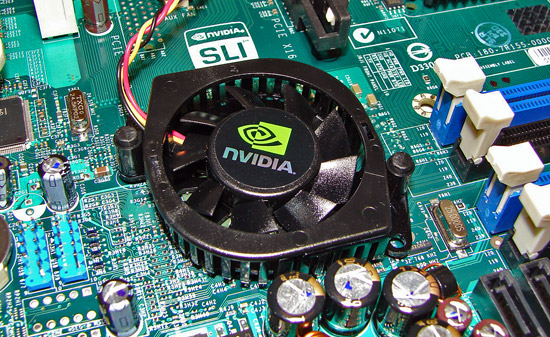
One of the last options to go is the third physical PCI Express x16 slot that operated at x8 speeds electrically. While the primary purpose for this slot centered on adding a third graphics card for physics acceleration that is still not available, it will be missed by users who had x4 or x8 devices such as PCI Express based RAID controller cards. The remaining differences between the boards is the lack of a passive cooling solution, LED post code display, onboard power and reset buttons, and speaker. Last, but by no means least, is an option reduced BIOS that is designed to offer just enough options to overclock the board to a certain degree, but it is missing just enough options to frustrate most users who will be purchasing this board based on its performance capabilities.
This leads us into today's performance review of the EVGA 680i LT SLI. In our article today we will briefly go over the board layout and features, provide a few important performance results, and discuss our findings with the board. We will provide further in-depth performance results of this product in a later article. With that said, let's take a quick look at this interesting board and see if it lives up to its hype.
It was several weeks before a motherboard manufacturer would offer a competing 680i solution. ASUS was the first non-reference board partner to offer competition to NVIDIA's reference design and it would take a few months before the likes of abit and Gigabyte were able to respond with their internal designs. We are still waiting on DFI's version to come to market and other motherboard manufacturers such as ECS and Biostar decided it was in their best interest to offer the reference board design that is built by Foxconn. The majority of NVIDIA's motherboard reference partners are actually heavily involved in the distribution of their graphics solutions with EVGA being the focal point of NVIDIA's reference program at this time.
The 680i SLI chipset has had a bumpy introduction with numerous issues being discovered and eventually fixed through a series of BIOS releases or new board revisions. The latest incarnation of the 680i SLI reference design from EVGA has solved our last remaining issues that concerned quad core overclocking performance. The non-reference partners have solid designs that have been hampered by immature BIOS releases but even those issues are starting to be resolved with the latest BIOS updates. While the 680i SLI based motherboards are finally on the right track from a performance and compatibility viewpoint, the pricing on these boards have been embarrassingly expensive to date. We have seen prices ranging from a low of $199 (EVGA 680i SLI board with rebate) to just over $400 for the ASUS Striker Extreme. On average, the majority of the 680i SLI boards sell in the $250 and up range.
With the 650i SLI boards just coming to market in volume and the 650i Ultra boards still not available, NVIDIA has had a difficult time in the Intel market from a competitive cost position. NVIDIA is starting to address that issue and is lowering the cost of entry into the mid to upper performance market with its new 680i LT SLI chipset. Like the 680i SLI chipset launch, this junior member of the 680i family will be available on a reference board design through a select number of partners as of this week. Once again, EVGA is one of the first partners to market with their 680i LT SLI motherboard priced at a more reasonable $199 (currently $174.99 with rebate). This is $50 less than the standard $249 MSRP for the 680i SLI reference boards but only $10 to $20 less than current street prices with rebates. This small difference in pricing could come back to haunt NVIDIA in the end, but we will have to see what street prices are before coming to any final conclusion.
Of course, before presenting performance results and discussing the complexities of this new reference design we need to first explain the differences between the 680i SLI and 680i LT SLI chipsets. We basically believe the 680i LT SLI SPP is a renamed 680i SLI SPP that has been feature reduced or more than likely neutered by the BIOS. The LT SPP carries the C55-P-N-A2 part number designation with its big brother being labeled with a C55-SLIX16N-A2 moniker. The real differences in the chipsets are in their choice of MCPs with the 680i LT utilizing the nForce 570 SLI MCP and the 680i SLI sporting the nForce 590 SLI MCP. It is always interesting to see how many times a recent NVIDIA MCP can be utilized in a different design or paired up with an ever increasing amount of SPP choices. We have to hand it to NVIDIA for having the ability to mix and match chipsets at will to create to new product line, but the constant renaming of the same chipsets has become tiresome and at times confusing.
With the chipset designations out of the way, let's see what the real differences are at this time. Both chipsets officially support front-side bus speeds up to 1333MHz so support for the upcoming Intel processors are guaranteed as is a certain amount of overclocking headroom. Both chipsets advertise "best-in-class" overclocking capability with the 680i SLI officially being termed "best" in this regard by NVIDIA. We think they are both equal but due to BIOS limitations we will probably never find out.
The 680i SLI offers full support for Enhanced Performance Profile (SLI-Ready) memory at speeds up to 1200MHz with the LT version only offering official 800MHz support. However, this only means you will have to tweak the memory speed and timings yourself in the BIOS, something most enthusiasts do anyway. We had no issue running our LT equipped board memory speeds up to 1275MHz so this feature deduction is not a real issue, although we wonder why they even offered limited support. Either do it all the way or don't do it all in our opinion.
Also missing in action is the Link Boost functionality that allows for an automatic 25% increase in the speed of the HyperTransport links that connect the SPP and MCP chipsets when utilized with an approved GeForce graphics solution. Although the performance improvements in benchmarks have been minimal to date, we have seen some minor increases in certain benchmarks with the 8800GTX cards. However, the GPU Ex option is available as is the QuickSync technology that improves memory performance when the memory is operating in sync mode. Once again, we have seen minimal performance differences in actual applications but every little bit helps.
The real differences between the chipsets are the missing features on the LT chipset. These include the loss of two USB ports (10 down to 8) and a Gigabit Ethernet port. The DualNet teaming feature is no longer available but will probably not be missed by the vast majority of users, nor will the loss of the second Ethernet port. However, the loss of two USB ports could cause issues with users who have several USB based peripherals.
One of the last options to go is the third physical PCI Express x16 slot that operated at x8 speeds electrically. While the primary purpose for this slot centered on adding a third graphics card for physics acceleration that is still not available, it will be missed by users who had x4 or x8 devices such as PCI Express based RAID controller cards. The remaining differences between the boards is the lack of a passive cooling solution, LED post code display, onboard power and reset buttons, and speaker. Last, but by no means least, is an option reduced BIOS that is designed to offer just enough options to overclock the board to a certain degree, but it is missing just enough options to frustrate most users who will be purchasing this board based on its performance capabilities.
This leads us into today's performance review of the EVGA 680i LT SLI. In our article today we will briefly go over the board layout and features, provide a few important performance results, and discuss our findings with the board. We will provide further in-depth performance results of this product in a later article. With that said, let's take a quick look at this interesting board and see if it lives up to its hype.


16 Comments
View All Comments
Stele - Wednesday, March 28, 2007 - link
It boils down to the engineering headroom put into the PWM design. Let's say the maximum supply current anticipated from a generation of CPUs is 50A (usually from datasheets and/or design guidelines from the CPU manufacturer). Motherboard designers can design their PWM to be just sufficient for this - most notably, the MOSFETs chosen may be those that can handle around 75A - or they can build some headroom in and choose MOSFETs capable of, say, 100A.
The former design philosophy saves cost, and after all it gets the job done. However, since the components would be running near their design limit, they would generate quite a bit of heat... especially during spikes of load and/or when new CPUs with even higher current draw (e.g. quad-core CPUs) show up.
The latter design philosophy is more expensive, but because the components would be running well below their rated spec, they fare much better in terms of thermal dissipation (and hence efficiency, as less power is lost as heat). The lower running temperatures also help improve the reliability of the components since less thermal stresses are present. Furthermore, when current loads increase - be it due to sudden load spikes and/or power-hungry CPUs and/or overclocking - they still have a lot of headroom, and so are able to handle the extra load without breaking a sweat. This results in better stability and again, lower heat dissipation compared to lower-spec'ed components at the same load.
In view of this, perhaps one other area that Anandtech could look at when reviewing motherboards is to have an IR thermometer handy (the ones that you can point and measure temperatures of surfaces remotely with) and perhaps measure the temperatures of the chipset and PWM (or at least the temperatures of their heatsinks) at idle and load. It may not be perfect (especially when heatpiped, and a hotter heatsink could also mean that the heat flow from the component to the heatsink is good due to good thermal contact) but imho at least it would give a useful ballpark figure.
Stele - Wednesday, March 28, 2007 - link
Pretty good review, critically assessing the chipset in light of theory (paper specs) as well as reality (actual value for money based on real-world prices and competiting products).IMHO, Nvidia's attempt to create a lower-cost version of the 680i SLI by limiting BIOS options and tossing the odd feature out (like passive chipset cooling and two USB/one network port) seems a little clumsy at best... Instead, I think the hybrid chipset combination used in, for example, the Asus P5N32-E SLI Plus is a more elegant solution. As this review demonstrated, the BIOS options do not necessarily cap the LT's overclocking capability enough to prevent it from being a threat to the 680i SLI's exclusive turf. Indeed, it might well turn out that the latter's sales would not be jeopardised by the LT anyway - not because of the arbitrarily imposed limitations, but because of the almost non-existent price difference between boards based on the two chipsets, considering the lost features.
Meanwhile, other reviews of the P5N32-E SLI Plus have noted that the MCP used is that from the AMD-platform 590 SLI chipset. I wonder if, other than the slight rearrangement of PCI-Express lanes, there are any real differences (e.g. revised/improved networking/disk controller engines etc) between the two MCPs? Or are these blocks nothing more than carried over directly from the 590 SLI? It would be great if Anandtech could look into that.
Lastly, a tiny note - it's a little amusing to note how it must be a bit pedantic to have to spell out the full name of the 'solid' capacitors used... at least Anandtech strives hard to get it right! :) Really, though, for the kind of 'solid' capacitors that we're talking about on most motherboards, "aluminium solid electrolytic capacitors" or even just "solid electrolytic capactitors" (vs. 'regular' (liquid) electrolytic) would do perfectly. Conductive polymer capacitors are generally (though not restricted to) the little rectangular ones such as the ones seen on Asus RoG boards as well as the P5N32-E SLI Plus. Just a thought :)
yyrkoon - Wednesday, March 28, 2007 - link
Well, about the capacitors, I know as per some OEM, anandtech was calling them 'solid state capacitors', which you sound like you know enough about electronics to know this is wrong. Anyhow, several readers, including myself called 'foul', and there you have it . . .JarredWalton - Wednesday, March 28, 2007 - link
There were a few complaints when he used "solid capacitors", so I guess the full name is the safe way to go. LOLStele - Wednesday, March 28, 2007 - link
Oh very true! "Solid capacitors" and "solid state capacitors" (as yyrkoon rightly commented) are both commonly used on many hardware sites, and are both inaccurate. One reason for the repeated complaints, iirc, is that we were simply oscillating between one inaccurate term and another. :P"Solid electrolytic capacitors"... now that is perfectly acceptable, despite a difference of one word. The devil, as they say, is in the details. ;)
yyrkoon - Wednesday, March 28, 2007 - link
You did the right thing Jarred, you know how picky 'us' readers are ;)