The Era of Tera: Intel Reveals more about 80-core CPU
by Anand Lal Shimpi on February 11, 2007 5:44 PM EST- Posted in
- CPUs
With no Spring Intel Developer Forum happening this year in the US, we turn to the International Solid-State Circuits Conference (ISSCC) for an update on Intel's ongoing R&D projects. Normally we'd hear about these sorts of research projects on the final day of IDF, these days presented by Justin Rattner, but this year things are a bit different. The main topic at hand today is one of Intel's Tera-scale computing projects, but before we get to the chip in particular we should revisit the pieces of the puzzle that led us here to begin with.
Recapping Tera-Problems
At the Spring 2005 Intel Developer Forum, Justin Rattner outlined a very serious problem for multi-core chips of the future: memory bandwidth. We're already seeing these problems today, as x86 single, dual and quad core CPUs currently all have the same amount of memory bandwidth. The problem becomes even more severe when you have 8, 16, 32 and more cores on a single chip.
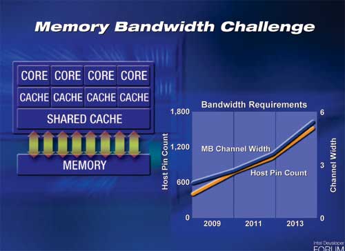
The obvious solution to this problem is to use wider front side and memory buses that run at higher frequencies, but that solution is only temporary. Intel's slide above shows that a 6-channel memory controller would require approximately 1800 pins, and at that point you get into serious routing and packaging constraints. Simply widening the memory bus and relying on faster memory to keep up with the scaling of cores on CPUs isn't sufficient for the future of microprocessors.
So what do you do when a CPU's access to data gets slower and more constrained? You introduce another level in the memory hierarchy of course. Each level of the memory hierarchy (register file, L1/L2/L3 cache, main memory, hard disk) is designed to help mask the latency of accessing data at the level immediately below it. The clear solution to keeping massively multi-core systems fed with data then is to simply put more memory on die, maybe an L4 cache perhaps?
The issue you run into here is that CPU die space is expensive, and the amount of memory we'd need to keep tens of cores fed is more than a few megabytes of cache can provide. Instead of making the CPU die wider, Intel proposed to stack multiple die on top of each other. A CPU die, composed of many cores, would simply be one layer in a chip that has integrated DRAM or Flash or both. Since the per-die area doesn't increase, the number of defects don't go up per die.
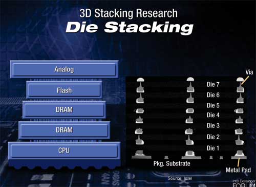
Memory bandwidth improves tremendously, as your DRAM die can have an extremely wide bus to connect directly to your CPU cores. Latency is also much improved as the CPU doesn't have to leave the package to get data stored in any of the memory layers.
Obviously there will still be a need for main memory, as Intel is currently estimating that a single layer could house 256MB of memory. With a handful of layers, and a reasonably wide external memory bus, keeping a CPU with tens of cores fed with data now enters the realm of possibility.
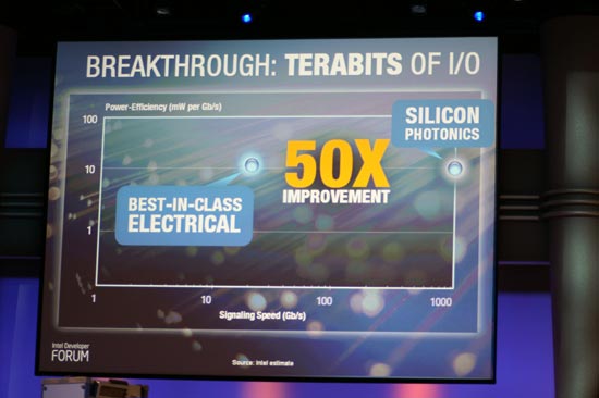
A year and a half later, Rattner was back but this time he was tackling another aspect of the era of tera - bus bandwidth. Although 3D die stacking will help keep many cores on a single die fed with data, the CPU still needs to communicate with the outside world. FSB technology, especially from Intel, has remained relatively stagnant over the past several years. If we're talking about building CPUs with tens of cores, not only will they need tons of memory bandwidth but they'll also need a very fast connection to the outside world.
Intel's research into Silicon Photonics has produced a functional hybrid silicon laser demonstrated at the Intel Developer Forum late last year. The idea is that optical buses can offer much better signaling speed and power efficiency than their electrical equivalents, resulting in the ideal bus for future massively multi-core CPUs.
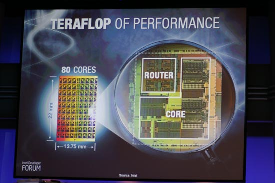
Justin Rattner's keynotes talked about some of Intel's Tera-scale projects, with 3D die stacking delivering terabytes of bandwidth needed for the next decade of CPUs and silicon photonics enabling terabits of I/O for connecting these CPUs to the rest of the system. The final vector that Rattner spoke about, was delivering a teraflop of performance. The CPU Rattner spoke of was a custom design by Intel that featured 80 cores on a single die, and today Intel revealed a lot more about its Teraflop CPU, the architecture behind it and where it fits in with the future of Intel CPUs.


25 Comments
View All Comments
Navitron - Monday, February 12, 2007 - link
In the words of bill gates "No one will need more than 637 kb of memory for a personal computer." You sound just like him :P Don't bash the technology just because "right now" we don't need it. But what about in 10-20 years, you still think your core 2 duo is gonna cut it in 15 years? Can a IBM 80386 run doom 3? will todays AMD and Intels run -insert game here- 10 years from now.So don't assume just because we don't need it now doesn't mean we wont need it in 3 years.
cscpianoman - Sunday, February 11, 2007 - link
The average consumer might not need it, but large industries will be grabbing at these things faster than you can imagine. Think of health care, for example, the trend is to move towards genetic manipulations/prescreening. These industries want to download a person's entire genetic information, process it, and return it to you with the results of Alzhiemer's, cancer, and heart problems in a matter of minutes. Furthermore, the entertainment industry would love to create more special effects and render them that much faster. I'm sure if they could Pixar would already be placing an order for these. There are hundreds of applications out there that require the power and capability of multi-cores. Sure the consumer may not need it, but the consumer only accounts for less than approx. 5% of what Intel, AMD or whoever makes.mino - Sunday, February 11, 2007 - link
They need it (to sell). Period.Justin Case - Sunday, February 11, 2007 - link
In other words, Intel is doing the same that IBM and AMD (with Cell and Torrenza + Fusion), only with some made-up numbers and more Powerpoint charts. Unless they vastly improve their compilers' paralellization, or come up with a full suite of software optimized for multi-core chips (80? It's hard enough to take full advantage of 4!), this will remain something that "can be done", but which most people will have no use for.joex444 - Sunday, February 11, 2007 - link
attack switch