Intel Demonstrates new 45nm Transistors and Conroe's Successor
by Anand Lal Shimpi on January 27, 2007 12:00 AM EST- Posted in
- CPUs
More Efficient Transistors
The basic function of a transistor as found in modern day microprocessors is to act as a switch with two states: on and off. When the transistor is on, current is allowed to flow from one terminal to the other (source to drain), and when it is off current shouldn't flow. Making enough current flow when it should and minimizing the amount that flows when it shouldn't is one of the major hurdles to making smaller transistors that run cooler/faster.
Below we have a typical CMOS transistor diagramed and labeled:
![]()
The voltage present at the Gate and the Source will determine whether or not current will flow in the transistor. Intel's 45nm process makes significant changes to two of the components in this transistor diagram: the gate electrode and the gate dielectric.
You can probably guess that as transistors get smaller, all of the parts of the transistor get smaller as well. The problem is that when some of these features get too small, they start behaving inappropriately. Case in point is the gate dielectric; with Intel's 90nm and 65nm processes, the gate dielectric was shrunk to a thickness of 1.2nm - the equivalent of about 5 atoms. The benefit of a very thin gate dielectric is that it increases the gate field effect, which increases drive current and reduces Source-drain leakage current. However, with such a thin gate dielectric electrons can tunnel directly through the layer and show up as leakage current - in other words, current would flow when it was not supposed to, translating into power wasted. On an individual transistor scale it's not such a big deal, but when you keep in mind that Penryn will have around 410 million of these transistors (820 million for quad-core) the leakage current/power draw does add up.
At 1.2nm, the gate oxide/gate dielectric in Intel's 90nm and 65nm transistors was as thin as Intel could make it without losing a great deal of power due to gate oxide leakage current. In order to make the move to 45nm Intel had to do something to thin the gate oxide without drastically increasing gate oxide leakage current.
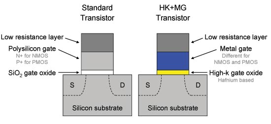
Intel solved the gate oxide leakage problem by replacing the SiO2 gate dielectric with a material that has a higher k-value, in this case a Hafnium based material. A high-k dielectric here actually increases drive current at the same thickness as the previous SiO2 dielectric, while reducing gate leakage as well. Intel isn't disclosing how thick the Hafnium gate dielectric layer is in its 45nm transistors, but we do know that it is thicker than the 1.2nm SiO2 gate dielectric used in previous 90nm and 65nm transistors.
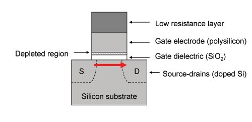
The second problem Intel is addressing with its 45nm transistors is a fundamental issue with the polysilicon gate electrode. The role of the gate electrode is important as it is what enables current to be driven through the transistor and as such it plays a role in how much current can be delivered. The polysilicon material that the gate electrode is made of has a tendency to form a region of depleted conducting carriers at the bottom of the gate, which reduces the drive strength of the transistor (less current flows when it needs to).
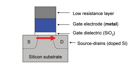
Intel's new 45nm transistors solve this problem by replacing the polysilicon gate electrode with a metal gate electrode, which completely eliminates the depleted region thus increasing the drive current.
Intel has been researching this High-k + Metal Gate (HK+MG) combination in transistors for a handful of years now, with hundreds of material options for metal gate electrodes and high-k dielectrics. The actual combination of high-k and metal gate material isn't being disclosed at this time, most likely to protect Intel's research and maintain the manufacturing advantage as long as possible. Intel expects that no other company will have HK+MG transistors until they reach 32nm or later.
The tangible advantages of these changes in materials in combination with the smaller 45nm process are quite large. According to Intel, the move from 65nm to 45nm yields a 30% reduction in transistor switching power because of the simple fact that smaller transistors have less parasitic capacitance and require less power to switch on and off.
Because of the combination of a high-k dielectric and the metal gate electrode, Intel is quoting a greater than 20% improvement in switching speed compared to its 65nm transistors. At the same speed as its 65nm transistors, there's a greater than 5x reduction in source-drain leakage power and a greater than 10x reduction in gate oxide leakage power; the latter is due entirely to the use of a high-k dielectric in the transistor. The end results of all of this are more power efficient processors, the first of which we should see by the end of this year.


59 Comments
View All Comments
Viditor - Tuesday, January 30, 2007 - link
OK...I choose Barcelona!
God I love these macho/nerd games...it takes me bake to my College days of D&D with Tequila shooters! (just be careful with that Intel +5 Vorpal Blade though!)
Huh? The stumbling block for scaling is Intel's platform (FSB)...
verndewd - Sunday, January 28, 2007 - link
lets make it fair and get a 65nm firstgen intel D900 series ,ultimately thats where the real comparison is at.(dont you wish it were that simple? hehehe)unfortunately Thats not the current market due to amd transitioning later than intel.The new york times said 9 months,but the first 65nm intels arrived late in 05.How is that for curious?
archcommus - Saturday, January 27, 2007 - link
Yeah, don't be a fanboy, buy whatever is the best purchase. My area of concern is that if AMD won't be delivering on par with Intel, it allows Intel to charge a price premium UNLIKE this past summer where we were lucky to see fierce price wars. If Intel gets too far ahead it could very well go back to the old days of Intel being the expensive mainstream chip and AMD being the cheaper choice for the DIYer.Regs - Saturday, January 27, 2007 - link
All I see is Intel advancement and AMD's foggy future.SunAngel - Saturday, January 27, 2007 - link
murder by numberssmn198 - Monday, January 29, 2007 - link
Also, the Intel Xeon ad appears on top of the article text. Really need to get my ad removing plug-in installed again.
bombledmonk - Monday, January 29, 2007 - link
it's 100mm^2, not 100mmx100mm. same for the 50mm^2bombledmonk - Monday, January 29, 2007 - link
whoops, wrong quote, and it had been answered below...shaunmarsh - Saturday, July 28, 2012 - link
This article is very good & informative.I have gain so much information from this blog.I like your blog.Thanks for the post.I am waiting for your new post.