Intel Demonstrates new 45nm Transistors and Conroe's Successor
by Anand Lal Shimpi on January 27, 2007 12:00 AM EST- Posted in
- CPUs
Yields and Manufacturing
Intel is sharing its usual vague data on yields at 45nm, but at least this time we get pretty good reference points to previous manufacturing processes. The graph below shows defect density as a function of time; you should keep in mind that processors generally don't start shipping until the very bottom of these curves in order to make the economics work for the CPU maker.
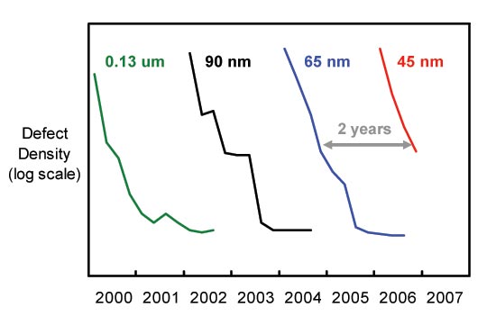
As you can see, 45nm is on a curve very similar to that of Intel's 65nm process, which means that things are on track for a smooth introduction later this year barring any unforeseen issues.
Intel attributed the rough patches in the 90nm trend to difficulty associated with building the first strained silicon transistors and using low-k interconnect dielectrics. By comparison, 65nm and 45nm appear to be much smoother sailing.
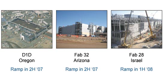
By the end of this year the first 45nm chips will be built at two 300mm Intel fabs: D1D in Oregon and Fab 32 in Arizona. Starting in the first half of 2008, Fab 28 in Israel will begin producing 45nm parts and should reach full capacity by the end of the year.
Final Words
It's very rare to get this much information out of Intel this far in advance of an actual product launch, but we're not complaining. By the middle of this year, AMD will launch its next-generation microarchitecture that will hopefully be a far better competitor to Intel's Core 2 processors. But before the year is out, Intel will respond yet again with its Penryn family of processors. We're unsure exactly what segments will be targeted first with Penryn, but by sometime in 2008 you should be able to get Penryn based notebooks, desktops and servers.
The inevitable comparison to AMD's progress on 45nm has to be made, but at this point we don't know too much. AMD revealed its 45nm SRAM test vehicle about three months after Intel did last year, with a slightly larger SRAM cell size (0.370 um^2 vs. 0.346 um^2 for Intel). The main focus for AMD at this point is the transition to 65nm; we're finally starting to see Brisbane cores available for purchase, but the highest clock speed offerings are still built on 90nm.
For Intel, we see continued strengthening and a roadmap that has a lot of promise. Penryn should be out sometime in the second half of this year, followed by a brand new architecture under the codename Nehalem. Nehalem will also be the first time we get to see an architecture change post-Core 2 under Intel's new tick-tock model of introducing new architectures every two years. It's quite possible that in the next two years Intel will have made the CPU industry far more exciting than it has been in the previous five (Core 2 launch withstanding).


59 Comments
View All Comments
tygrus - Sunday, January 28, 2007 - link
100mm^2 is twice the area as 50mm^2.100mm^2 means the mm is squared not the 100.
10mm x 10mm = 100mm^2
5mm x 10mm = 50mm^2
lopri - Saturday, January 27, 2007 - link
I am more interested in the long-awaited introduction of integrated memory controller from Intel CPU. IIRC, it's supposed to happen with 45nm process, which makes me curious whether Nehalem will be the one. This will likely happen in parallel with HSI, or High Speed Interconnect, which is supposed to be compatible with PCI-Express 2. (How that can be done - beats me) Nehalem might as well be 'simply' Core 2 Duo + IMC as Hammer was Athlon XP + IMC.While this is obviously Intel's PR piece, it is an undeniable truth that AMD doesn't even have anything for such. It's foolish to think that AMD wouldn't be bragging had they have made an advance like this.
A good news for AMD is that the processing power for desktop has, to my eyes, reached to the point that it's sufficient for majority of daily computing for forseable future. In other words, majority of people will not likely take advantage of any more computing power (be it speed or multitasking) than what current CPUs can process. I wonder AMD will turn to a totally different direction from this hopeless speed race.
IntelUser2000 - Sunday, January 28, 2007 - link
HSI?? High Speed Interconnect?? That's a new one. No, its CSI, and it stands for Common System Interface, which was originally named because it was supposed to bring socket compatibility between Itanium and Xeon, or at least the electrical part of it.
lopri - Sunday, January 28, 2007 - link
Got me there. Yah it's CSI. Thanks for the correction.MadBoris - Saturday, January 27, 2007 - link
Maybe I am missing something here, but where is the chipset information.Is this going to be on a new chipset, or 775 compatible?
Knowing Intel, it's a new chipset, they love to stimulate the economy (their economy) with new chipsets all the time.
Any word?
Groovester - Saturday, January 27, 2007 - link
Due to HK+MG's 20% higher switching rate and much lower leakage currents, shouldn't we expect ("more power efficient processors") both higher clock speeds AND lower TDP, even with a slightly higher transistor count?IntelUser2000 - Sunday, January 28, 2007 - link
No. First thing is the recent roadmaps shown by HKEPC say it doesn't lower power, part of the reason is to increase yields, the other has to be clock speeds.
(If you want to read further, go ahead, but it tends to be long)
It does present much lower leakage, but there is a caveat: "Intel is quoting a greater than 20% improvement in switching speed compared to its 65nm transistors. At the same speed as its 65nm transistors, there's a greater than 5x reduction in source-drain leakage power and a greater than 10x reduction in gate oxide leakage power"
The source-drain is the reason for leakage power when the transistor is active(meaning its on), and gate oxide leakage power is for idle. Read the second sentence carefully: "At the same speed as its 65nm transistors...
It means if Intel wants to take advantage of the 20% increase in clock speed, they'll likely have to forgo the reduction in active leakage power. Contrary to what most news sites wants you to believe, leakage isn't of a big problem as they want you to believe(most of the reason is that they want hits to the webpage), especially on a power optimized CPU like Conroe. The exponential leakage increase every shrinking process would have been true if the companies like Intel did nothing about it. Of course they can't allow that to happen and added their own optimizations and enhancements. Its not a complete elimination either, but a 5x reduction.
If they want to keep the 65W, we'll have to base it on the E6700, which is at 2.66GHz. With 1333MHz FSB, I can see mainstream dual core devices clock at 3.66/3.83GHz. Since it seems Intel is using a "family TDP", the 65W figure would likely have to be made to fir the 3.66/3.83GHz part. They may be able to tweak it higher and go 4.0GHz or lower power, but that tweaks will probably be seen on the Nehalem derivatives.
2.66GHz x (20% faster) = 3.2GHz
30% lower power = 0.7 But
0.7 x 1.44(going beyond 3.2GHz will require greater than nominal voltages, which means more power. But faster clock speeds also mean more power. 20% higher voltage x 20% higher clock = 44% higher power)~1.00
Sure some of you guys like to lower voltages below nominal and don't overclock, but possible sacrifice in stability won't be seen as good for the corporate market and Intel generally.
So approximately same power consumption
Now if you kept up to the roadmaps you might say, what about the 1333MHz 3.0GHz parts that's also said to be at 65W?? First, look at the X6800 with 75W TDP. Well, since the 3.0GHz/1333MHz FSB parts come a year later after Conroe, Intel will have time to tweak it.
IntelUser2000 - Saturday, January 27, 2007 - link
If we derive clock speed numbers from Anandtech's Spring IDF 2005 article about Presler, we should be able to come up with a similar number :).http://www.anandtech.com/showdoc.aspx?i=2362">http://www.anandtech.com/showdoc.aspx?i=2362
"It looks like the chip was running at 2.0GHz, which isn't too impressive in itself, until you remember that we're talking about a 65nm processor here whose launch is over a year away."
45nm Quad core Desktop parts running at 1.86GHz
45nm Dual core desktop parts running at 2.13GHz
Now Presler came with 3.6GHz for the mainstream(Pentium D 960) and 3.73GHz with the enthusiast(Pentium Extreme Edition 3.73GHz). If we apply similar increase between prototype and final product, we get:
45nm Quad core desktop: 3.46GHz @ 1066MHz FSB/3.5GHz @ 1333MHz FSB(45nm parts support half step dividers)
45nm Dual core desktop: 4.0GHz @ 1333MHz FSB
Since the TDP is not supposed to go down, we can expect all the power headroom to be translated to clock speed. The estimations also match the roadmaps.
Staples - Saturday, January 27, 2007 - link
A price drop. It is ridiculous that C2Ds have not dropped a cent since they came out 6+ months ago.MarkM - Saturday, January 27, 2007 - link
http://www.nytimes.com/2007/01/27/technology/27chi...">http://www.nytimes.com/2007/01/27/techn...63262&am...