Intel Demonstrates new 45nm Transistors and Conroe's Successor
by Anand Lal Shimpi on January 27, 2007 12:00 AM EST- Posted in
- CPUs
Conroe has a Son: Introducing Penryn
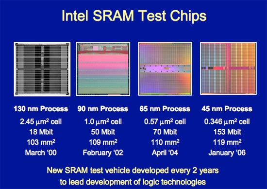
Intel announced the first working high-k + metal gate transistors back in 2003. By 2006 it had built an SRAM test vehicle (a wafer full of nothing but cache and some control/test logic) using the new transistors to work out most of the kinks in the manufacturing process.
Today, Intel is announcing that its first full CPU built using the new 45nm high-k + metal gate transistors is not only up and running, but it has also booted four OSes. The very first packaged Penryn silicon from the very first wafer booted Windows Vista, Mac OS X, Windows XP and Linux on the first try.
The picture below is of Intel's validation team after they successfully booted Penryn on the above OSes. The chips arrived in the lab at around 1AM and by 3AM they were up and running. If you're concerned, that's sparkling cider in those glasses and not champagne; alcohol is not allowed on Intel's campus, as it tends not to bring out the best in CPU designs, although it does make benchmark scores look infinitely higher.

It's a fairly big accomplishment to have first silicon working this well, but Intel has had a number of successful first spins in recent history. Generally by the time you're making your first CPUs, you've got the majority of the manufacturing defects worked out thanks to your SRAM test vehicle, so any problems with the first silicon are usually due to errors in the design or in the masks.
Intel also proudly sent us a shot of the 45nm Penryn die:
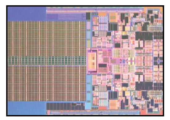
This version of Penryn is dual-core, and the first quad-core Penryn chips will simply be two of these on a single package, although later on we may see a single-die solution. At 410 million transistors, we expect a dual-core Penryn to have a 6MB shared L2 cache (up from 4MB in Conroe). The logic part of the Penryn core will be mostly evolutionary from Conroe, but do expect additional functionality and performance from more than just a larger cache.
If we assume that 288M transistors (6T SRAM) will be used by the 6MB cache, that leaves 122M transistors for L1 cache and the rest of the core. Applying the same calculation to Conroe gives us 99M transistors left over, meaning that there are roughly 23% more core-logic, control and L1 transistors being used in Penryn than in Conroe.
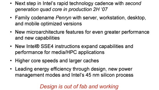
What that additional functionality will be is up in the air at this point, but you can expect SSE4 support to occupy a chunk of those transistors. At 45nm Intel should also be able to ramp up clock speed, so expect to see Penryn debut at over 3GHz easily. Given how overclockable Conroe turned out to be, we wouldn't be too surprised to see Penryn scale very well.
And the last bit of Penryn information Intel is letting out today is that it demonstrated Penryn up and running actual applications at a press briefing in Santa Clara on January 25th. There were five Penryn systems configured and clocked as follows:
1) 45nm dual core mobile processor in a notebook with Microsoft Vista running Microsoft Office 2003 applications.
2) 45nm dual-core desktop processor running high definition video content (1080P) under Microsoft Vista. 2.13 GHz
3) 45nm quad-core desktop processor running Ubisoft Rainbow Six Las Vegas game under Microsoft Vista. 1.86 GHz
4) Two 45nm dual-core processors running Glaze Workstation application under Microsoft Windows 2000 Advanced Server. 2.13 GHz
5) Two 45nm quad-core processors encoding a video in Adobe Premier under Microsoft Vista. 2.13 GHz
All of the systems were air-cooled using normal heatsink/fan units. Unfortunately Intel wouldn't share any benchmarks or more details of the systems other than what software they were running.
At this stage in the game it's normal to see clock speeds much lower than final shipping silicon, but this is the first time that Intel has been so forthcoming with clock speed data this far before launch. What we're seeing is a far more proud and confident Intel, and honestly it has every reason to be given the recent successes of Core 2 and promise of Penryn.


59 Comments
View All Comments
tygrus - Sunday, January 28, 2007 - link
100mm^2 is twice the area as 50mm^2.100mm^2 means the mm is squared not the 100.
10mm x 10mm = 100mm^2
5mm x 10mm = 50mm^2
lopri - Saturday, January 27, 2007 - link
I am more interested in the long-awaited introduction of integrated memory controller from Intel CPU. IIRC, it's supposed to happen with 45nm process, which makes me curious whether Nehalem will be the one. This will likely happen in parallel with HSI, or High Speed Interconnect, which is supposed to be compatible with PCI-Express 2. (How that can be done - beats me) Nehalem might as well be 'simply' Core 2 Duo + IMC as Hammer was Athlon XP + IMC.While this is obviously Intel's PR piece, it is an undeniable truth that AMD doesn't even have anything for such. It's foolish to think that AMD wouldn't be bragging had they have made an advance like this.
A good news for AMD is that the processing power for desktop has, to my eyes, reached to the point that it's sufficient for majority of daily computing for forseable future. In other words, majority of people will not likely take advantage of any more computing power (be it speed or multitasking) than what current CPUs can process. I wonder AMD will turn to a totally different direction from this hopeless speed race.
IntelUser2000 - Sunday, January 28, 2007 - link
HSI?? High Speed Interconnect?? That's a new one. No, its CSI, and it stands for Common System Interface, which was originally named because it was supposed to bring socket compatibility between Itanium and Xeon, or at least the electrical part of it.
lopri - Sunday, January 28, 2007 - link
Got me there. Yah it's CSI. Thanks for the correction.MadBoris - Saturday, January 27, 2007 - link
Maybe I am missing something here, but where is the chipset information.Is this going to be on a new chipset, or 775 compatible?
Knowing Intel, it's a new chipset, they love to stimulate the economy (their economy) with new chipsets all the time.
Any word?
Groovester - Saturday, January 27, 2007 - link
Due to HK+MG's 20% higher switching rate and much lower leakage currents, shouldn't we expect ("more power efficient processors") both higher clock speeds AND lower TDP, even with a slightly higher transistor count?IntelUser2000 - Sunday, January 28, 2007 - link
No. First thing is the recent roadmaps shown by HKEPC say it doesn't lower power, part of the reason is to increase yields, the other has to be clock speeds.
(If you want to read further, go ahead, but it tends to be long)
It does present much lower leakage, but there is a caveat: "Intel is quoting a greater than 20% improvement in switching speed compared to its 65nm transistors. At the same speed as its 65nm transistors, there's a greater than 5x reduction in source-drain leakage power and a greater than 10x reduction in gate oxide leakage power"
The source-drain is the reason for leakage power when the transistor is active(meaning its on), and gate oxide leakage power is for idle. Read the second sentence carefully: "At the same speed as its 65nm transistors...
It means if Intel wants to take advantage of the 20% increase in clock speed, they'll likely have to forgo the reduction in active leakage power. Contrary to what most news sites wants you to believe, leakage isn't of a big problem as they want you to believe(most of the reason is that they want hits to the webpage), especially on a power optimized CPU like Conroe. The exponential leakage increase every shrinking process would have been true if the companies like Intel did nothing about it. Of course they can't allow that to happen and added their own optimizations and enhancements. Its not a complete elimination either, but a 5x reduction.
If they want to keep the 65W, we'll have to base it on the E6700, which is at 2.66GHz. With 1333MHz FSB, I can see mainstream dual core devices clock at 3.66/3.83GHz. Since it seems Intel is using a "family TDP", the 65W figure would likely have to be made to fir the 3.66/3.83GHz part. They may be able to tweak it higher and go 4.0GHz or lower power, but that tweaks will probably be seen on the Nehalem derivatives.
2.66GHz x (20% faster) = 3.2GHz
30% lower power = 0.7 But
0.7 x 1.44(going beyond 3.2GHz will require greater than nominal voltages, which means more power. But faster clock speeds also mean more power. 20% higher voltage x 20% higher clock = 44% higher power)~1.00
Sure some of you guys like to lower voltages below nominal and don't overclock, but possible sacrifice in stability won't be seen as good for the corporate market and Intel generally.
So approximately same power consumption
Now if you kept up to the roadmaps you might say, what about the 1333MHz 3.0GHz parts that's also said to be at 65W?? First, look at the X6800 with 75W TDP. Well, since the 3.0GHz/1333MHz FSB parts come a year later after Conroe, Intel will have time to tweak it.
IntelUser2000 - Saturday, January 27, 2007 - link
If we derive clock speed numbers from Anandtech's Spring IDF 2005 article about Presler, we should be able to come up with a similar number :).http://www.anandtech.com/showdoc.aspx?i=2362">http://www.anandtech.com/showdoc.aspx?i=2362
"It looks like the chip was running at 2.0GHz, which isn't too impressive in itself, until you remember that we're talking about a 65nm processor here whose launch is over a year away."
45nm Quad core Desktop parts running at 1.86GHz
45nm Dual core desktop parts running at 2.13GHz
Now Presler came with 3.6GHz for the mainstream(Pentium D 960) and 3.73GHz with the enthusiast(Pentium Extreme Edition 3.73GHz). If we apply similar increase between prototype and final product, we get:
45nm Quad core desktop: 3.46GHz @ 1066MHz FSB/3.5GHz @ 1333MHz FSB(45nm parts support half step dividers)
45nm Dual core desktop: 4.0GHz @ 1333MHz FSB
Since the TDP is not supposed to go down, we can expect all the power headroom to be translated to clock speed. The estimations also match the roadmaps.
Staples - Saturday, January 27, 2007 - link
A price drop. It is ridiculous that C2Ds have not dropped a cent since they came out 6+ months ago.MarkM - Saturday, January 27, 2007 - link
http://www.nytimes.com/2007/01/27/technology/27chi...">http://www.nytimes.com/2007/01/27/techn...63262&am...