AMD's 65nm Preview Part 2 - The Plot Thickens (Updated with Information from AMD)
by Anand Lal Shimpi on December 21, 2006 12:12 AM EST- Posted in
- CPUs
Updated: Page 3 has been updated to include an official AMD response on the Brisbane performance issues we've been seeing. AMD confirmed an increase in L2 cache latency in order to support a move to larger cache sizes in the future, which may or may not happen. The rest of the article remains unchanged.
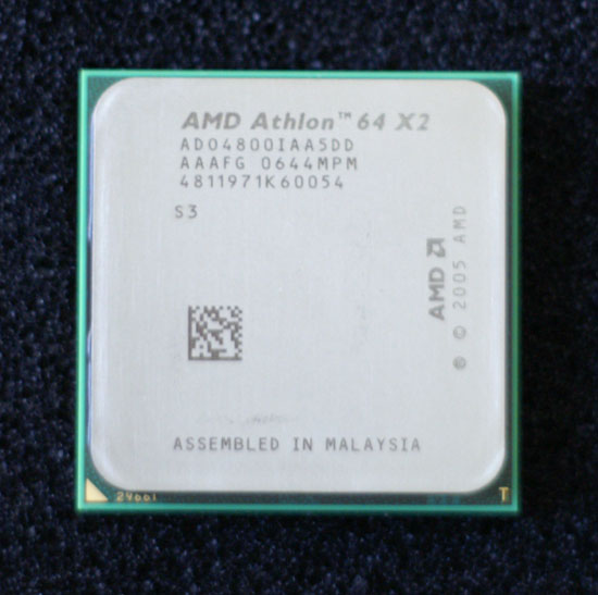
Last week AMD sent us samples of its first 65nm processors, codenamed Brisbane, and it was a step towards being competitive with Intel again. The 65nm shrink yielded AMD's most efficient desktop processor to date, but it's still a far cry away from what Intel is able to accomplish with its Core 2 processors.
Although they won't be available until sometime next year, a closer look at AMD's 65nm lineup reveals an interesting fact. Until recently, AMD would differentiate between subsequent model numbers by clock speed and cache size, alternating between the two. So while the Athlon 64 X2 4600+ and 4800+ both ran at 2.4GHz, the latter had twice the L2 cache per core at 1MB. After Intel's Core 2 launch, AMD killed all non-FX 1MB L2 parts, resulting in a processor lineup that was mostly segregated according to clock speed. (Of course they then added the X2 5200+ and 5600+ back into the mix....) With the move to 65nm, AMD is once again introducing model numbers that it had killed off before, but without playing with L2 cache sizes; instead, AMD is breaking with recent tradition and implementing non-integer clock multipliers for these "new" in-between speeds. The table below explains it all:
| CPU | Clock Multiplier | Clock Speed |
| AMD Athlon 64 X2 5000+ EE | 13.0x | 2.6GHz |
| AMD Athlon 64 X2 4800+ EE | 12.5x | 2.5GHz |
| AMD Athlon 64 X2 4600+ EE | 12.0x | 2.4GHz |
| AMD Athlon 64 4400+ EE | 11.5x | 2.3GHz |
| AMD Athlon 64 X2 4000+ EE | 10.5x | 2.1GHz |
We didn't mention this in the original article, but all of AMD's 65nm CPUs are considered to be Energy Efficient (denoted by the letters EE in the table above). With its 90nm chips, AMD specifically selected lower voltage parts to be labeled as Energy Efficient, but right now all 65nm parts are. For the sake of simplicity, especially as we compare to older EE parts, we will simply refer to these chips as 65nm chips.
Note that the 65nm 4800+, 4400+ and 4000+ all use non-integer clock multipliers, a first for the Athlon 64 line. The implications for the end user are relatively minor, although it does mean that the model numbers will translate into more consistent performance graduations. In the past, having two chips running at the same clock speed but with different cache sizes meant that one would be faster only in those applications that could use the extra cache.
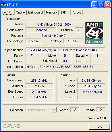
Despite support for non-integer clock multipliers, all AMD chips still only support integer memory dividers, meaning that only CPUs with even CPU multipliers can run at DDR2-800. All odd clocked (5000+) and half-clocked processors (4800+, 4400+, 4000+) run at a slower than DDR2-800 speed, even when set to DDR2-800 in the BIOS. AMD wouldn't discuss whether or not this would be addressed in the future, but if it is we'd have to wait for at least another silicon revision.
By now, none of this is new information, which brings us to why we're here today. In our original 65nm article we noticed a performance disparity between AMD's 65nm and 90nm processors, yet we had no official response from AMD as to why; today we have that answer. At the same time, we wanted to take a look at one of the half-multiplier chips and add it to our performance and power graphs, not to mention include some lower cost Intel CPUs per your requests. We've also got some more insight into the die sizes and power consumption figures we reported in our last article. In a sense, we're tying up loose ends with this piece, and shedding more light on AMD's 65nm cores than we originally did in our first, quick preview.


52 Comments
View All Comments
Schugy - Thursday, December 21, 2006 - link
Being able to sell more chips is not an argument for consumers but for AMD. Brisbane is not like Prescott - AMD has done a good job. Further development is needed but first 65nm units are running and are the basis for new architectures with increased transistor count.Yoshi911 - Thursday, December 21, 2006 - link
Hey all, I know that Socket 939 is obselete now but I think It'd be awesome if they'd make a 939 65nm core.. I still have my Opteron 144 at 3.1ghz on my Lanparty board and would love to see a core I could update to before the nextgen AMD achatecture makes it out.Anyone know if this is a possibilty??
Spoelie - Thursday, December 21, 2006 - link
get a 165 for 150$, overclock it to at least 2.8ghz and you have fx62 like performancethat's the best thing you will ever get on socket 939 I'm afraid, now and in the future.
peldor - Thursday, December 21, 2006 - link
Practically, it's never gonna happen. The market wouldn't be worth the effort.OcHungry - Thursday, December 21, 2006 - link
I don’t understand why anyone or any review expect stellar overclocking or performance from these 65nm’s?Did AMD promise any? No. AMD promised a transition to 65nm and on time. That’s what we all should expect and appreciate the successful transition.
Do you remember the first batch of Intel's 65nm Core 2’s? It was not as good as what you see today. Frankly I think AMD did much better in 65nm than Intel back then, and this first release is giving Core 2 due's matured chip a run for the money. After all the review here clearly shows AMD is on tract w/ 65nm’s performance per watt and energy consumption. Don’t forget its still K8 architecture competing w/ the latest and the greatest of Intel's.
IntelUser2000 - Thursday, December 21, 2006 - link
Which first batches?? The ones XS has been receiving far before the official Core 2 Duo release?? What's the OC that AT got??
http://www.anandtech.com/cpuchipsets/showdoc.aspx?...">http://www.anandtech.com/cpuchipsets/showdoc.aspx?...
X6800 went from 2.93GHz to 3.6GHz with default voltage. On a very good air cooler and voltage increased, it reached 4.0GHz.
E6700: 2.667GHz to 3.4 default, 3.9 highest
E6600: 4.0GHz highest
X6800 stock cooler highest: 3.4GHz
Tomshardware: X6800 to 3.46GHz
Xbitlabs: X6800 to 3.4GHz, 3.6GHz with +voltage
Brisbane 5000+
2.6GHz to 2.925GHz, on stock cooler, 1.475V.
It's not that bad for Brisbane IMO. It seems more like an architectural limitation than process or thermal limitation. Core 2 Duo still has ways to go and roadmaps sort of reflect it. Though the increase in L2 access latencies may mean it was done to increase the clock speed potential.
peldor - Thursday, December 21, 2006 - link
Going to 65nm shouldn't move you backwards in performance though. There's no excuse for that from the consumer's POV unless the price also goes down (certainly a possibility if yields are good).ydoucensor - Thursday, December 21, 2006 - link
could the increase in latencies have something to do with "trusted" computing and the need for attestation?fitten - Thursday, December 21, 2006 - link
Pure speculation, but the L2 latency increase may be a result of work going into the three level cache controller logic getting ready for K8L or whatever it's going to be.mino - Thursday, December 21, 2006 - link
My thoughts exactly.