Fall IDF 2006 - Day 1: Laser FSBs, more Alan Wake, Flash in Vista & DDR3
by Anand Shimpi & Cara Hamm on September 27, 2006 3:16 AM EST- Posted in
- Trade Shows
For the first IDF after Intel's Conroe launch you have to give Intel credit, the folks are trying their best to make things interesting. Earlier today we reported on Intel's 65nm ramp, transition to 45nm, Conroe/Woodcrest shipments and upcoming quad-core solutions among other things.
We're rounding out our first day's coverage with an update from the Intel labs on Silicon Photonics, more information on multi-threaded gaming in Remedy's upcoming thriller: Alan Wake, Intel's Robson technology for notebooks and the world's first demonstration of DDR3 memory on an unannounced Intel desktop chipset.
Silicon Photonics Interconnects: Coming to a Chip Near You
For the past five years, Intel has been hard at work on building a silicon laser. Using light as a medium for data transmission is nothing new, after all many high speed networks operate over fiber optic cable, however the idea of using light as an alternative to electrical signaling at the chip level is a bit more revolutionary.
Photonic signaling is in many ways superior to electrical signaling as you can get much higher bandwidths out of an optical bus than you can out of an electrical bus. As the number of CPU cores and their operating frequencies increase tremendously, the demands for a higher speed I/O interface will as well. There will come a time where sending electrical data over copper wires is no longer fast enough to keep up with the growing bandwidth needs of these processors, and it's at that point where we'll have to turn to another, higher bandwidth solution. Intel hopes that its research into Silicon Photonics will hold the key to that solution.
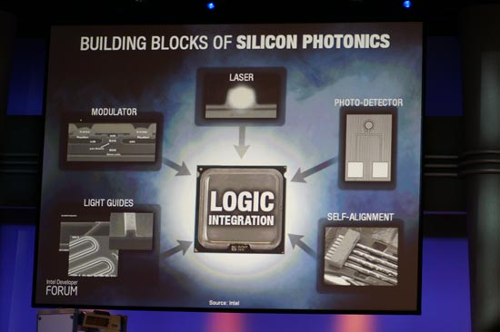
As we mentioned earlier, transmitting data using light has been around for ages, whether in the form of igniting a fire to mean "help!" or using light (or the absense of it) to represent binary data. The trick is being able to generate and use light entirely on silicon, because if you can do that, then you can use light to transmit data on die. In order to build silicon around optical interfaces you need to first be able to generate light on die itself, in other words you need to be able to generate light using electricity within the confines of a silicon chip.
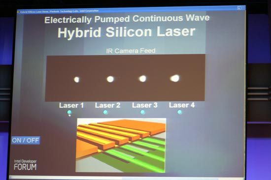
In the past, Intel's Silicon Photonics demonstrations have used externally generated light as a laser source and then worked on integrating the various other parts of the equation on silicon. Just recently, Intel demonstrated its first hybrid silicon laser that was made using standard silicon maufacturing techniques. The name hybrid silicon laser comes from the fact that the laser is produced from a combination of Indium Phosphide and standard silicon.
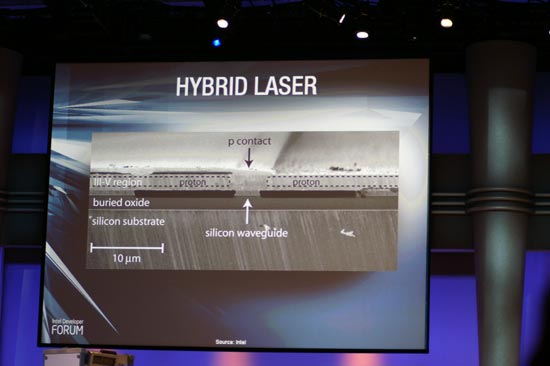
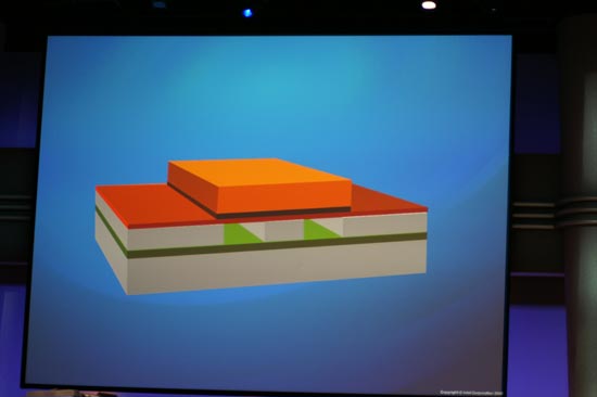
Wave guides are etched out of the silicon layer of the chip, allowing the eventual laser to be channeled, but in order to actually generate the light using electricity you need a compound that will produce light - in this case, it's Indium Phosphide (a III-V compound as it is produced using elements from the III and V columns of the periodic table).
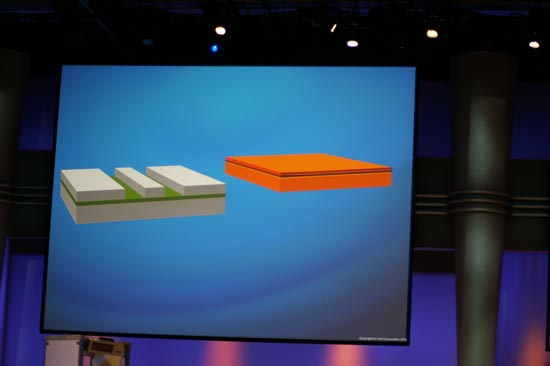
A layer of Indium Phosphide is created to be the same size as the silicon which the waveguides are carved out of.Both the silicon and InP are exposed to an oxygen plasma to create a glue-like layer, approximately 25 atoms thick, on both layers.
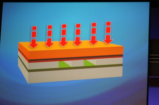
Then, the silicon and InP are fused together and channels are etched out of the top InP layer:
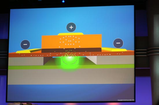
When you apply a charge across the InP layer, the electrons cause the InP to generate light that is then reflected into the waveguides in the silicon, thus creating a laser within silicon.
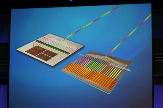
Being able to generate the laser on silicon is just one step of the whole process, but it is a very important one. With lasers generated, you can then encode binary data on and multiplex multiple lasers into a single output, offering tremendous bandwidth.
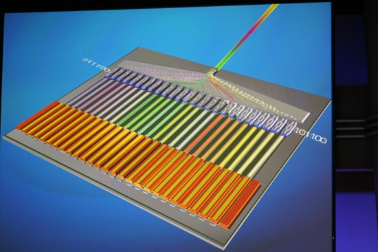
The data can then be sent over the single output to a de-multiplexer and decoder that would recover the original binary data and convert it back into electrical signals that could be used by regular silicon based processors:
Intel is still years away from being able to use any of this silicon photonics technology in a product, but progress is being made. Intel demonstrated its hybrid laser at IDF, simply showing that it works and was produced using conventional silicon manufacturing processes.
The apparatus below basically holds a hybrid laser chip, provides it with power and is placed next to an IR camera to detect the light produced by the chip:
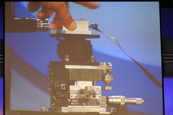
As you can see the chip does produce light, and Justin Rattner even slid his hotel keycard between the camera and the chip to confirm that the demo was live and that the chip was actually producing the light.
The implications of Intel's work in silicon photonics are tremendous, as it would allow Intel the bandwidth necessary to connect CPUs with tens or hundreds of cores to the outside world. While we're still years away from seeing this technology used in a product, we were glad to see Intel keep us updated on its progress.
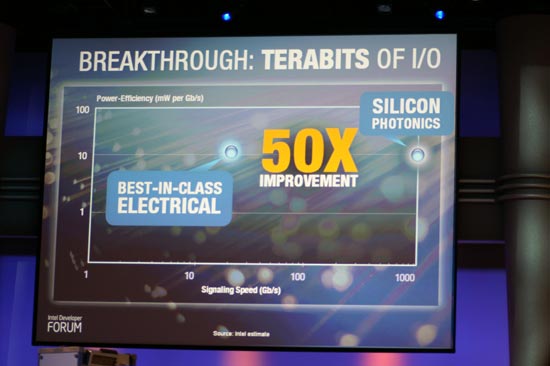
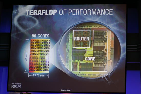
Alongside Intel's focus on silicon photonics to deliver what it is calling "Terabits of I/O", Justin Rattner also talked about being able to deliver Terabytes of bandwidth and Teraflops of performance for the future of Intel microprocessors. The Terabytes of bandwidth would come through the use of stacked die technology, which Rattner talked about at IDF six months ago. As a recap, stacked die technology could be used to create a layer of cache that would attach directly to a CPU in order to give it a very large, very high performance memory subsystem that was still quite low latency.
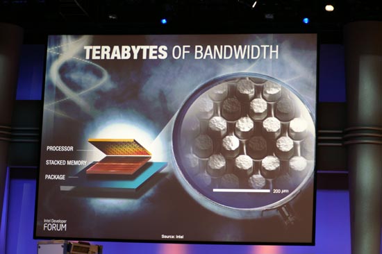
Intel's Teraflop CPU could theoretically use a stacked die approach to deliver the sort of memory bandwidth it would need to keep all 80 of its FP cores fed.


16 Comments
View All Comments
DigitalFreak - Wednesday, September 27, 2006 - link
Until at least 2008, I bet the VAST majority of multi-threaded games on the PC will be "ports" of Xbox 360 games.NullSubroutine - Wednesday, September 27, 2006 - link
what say you when AMD's inverted hyper-threading is available? the one that runs 1 thread on multiple cores. the reason why game developers have to start programming multithread games is because in the not to distant future all threads (including video) will be run via multi-cored cpu.johnsonx - Wednesday, September 27, 2006 - link
it's been stated numerous times that 'inverse' or 'reverse' hyper-threading is nothing more than a myth. No one even knows how it got started, but it may have been a misunderstanding of AMD's Dual Core Optimization utility.ShapeGSX - Wednesday, September 27, 2006 - link
"Reverse hyperthreading" is just not practical, nor would it give much of a boost in performance. It would take some major communication between cores during instruction fetch, instruction issue, and instruction retire.Why wouldn't it give much of a boost? As it is, with 4 issue processors like the Core 2 Duo, it is very hard to find a window of instructions in a program that the processor can issue in parallel. Even now, some execution units are empty during most clock cycles. So what would be the point of trying to do even more in parallel? You would just end up with more empty execution units, but now on 2 or more cores instead of just one.
This is why multithreading on processors was invented in the first place. It was to fill up empty execution units with work from other threads, which is inherently parallel and doesn't have dependencies.
NullSubroutine - Wednesday, September 27, 2006 - link
so like i was excited about the laser things. i cant wait till i can put those chips inside my mutated seabass (with attached laser also on their head) cybornetic brain. i will have frikin lasers galore!Hypernova - Wednesday, September 27, 2006 - link
Optical interconnects are perhapes the most important invention right behind IC itself. The next 10 years will be very exciting no doubt.