Intel's Core 2 Extreme & Core 2 Duo: The Empire Strikes Back
by Anand Lal Shimpi on July 14, 2006 12:00 AM EST- Posted in
- CPUs
The architecture is called Core, processor family is Core 2, the product names are Core 2 Duo and Core 2 Extreme. In the past we've talked about its architecture and even previewed its performance, but today is the real deal. We've all been waiting for this day, the day Intel lifts the last remaining curtain on the chip that is designed to re-take the performance crown from AMD, to return Intel to its days of glory.
It sure looks innocent enough:
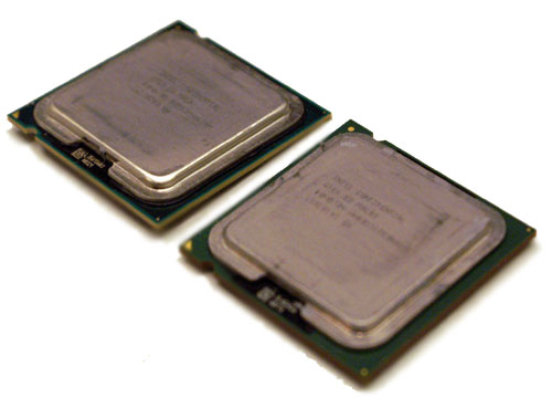
Core 2 Duo (left) vs. Pentium D (right)
What you see above appears to be no different than a Pentium D. Honestly, unless you flip it over there's no indication of what lies beneath that dull aluminum heat spreader.
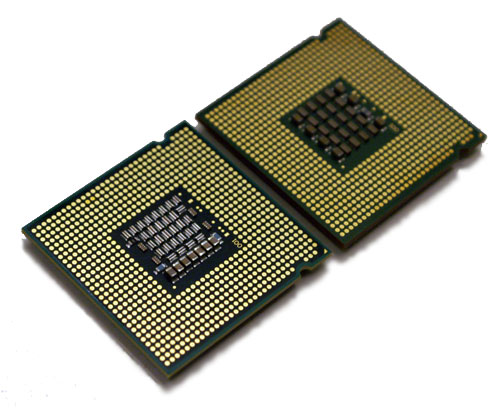
Core 2 Duo (left) vs. Pentium D (right)
But make no mistake, what you see before you is not the power hungry, poor performing, non-competitive garbage (sorry guys, it's the truth) that Intel has been shoving down our throats for the greater part of the past 5 years. No, you're instead looking at the most impressive piece of silicon the world has ever seen - and the fastest desktop processor we've ever tested. What you're looking at is Conroe and today is its birthday.
Intel's Core 2 launch lineup is fairly well rounded as you can see from the table below:
| CPU | Clock Speed | L2 Cache |
| Intel Core 2 Extreme X6800 | 2.93GHz | 4MB |
| Intel Core 2 Duo E6700 | 2.66GHz | 4MB |
| Intel Core 2 Duo E6600 | 2.40GHz | 4MB |
| Intel Core 2 Duo E6400 | 2.13GHz | 2MB |
| Intel Core 2 Duo E6300 | 1.86GHz | 2MB |
As the name implies, all Core 2 Duo CPUs are dual core as is the Core 2 Extreme. Hyper Threading is not supported on any Core 2 CPU currently on Intel's roadmaps, although a similar feature may eventually make its debut in later CPUs. All of the CPUs launching today also support Intel's Virtualization Technology (VT), run on a 1066MHz FSB and are built using 65nm transistors.
The table above features all of the Core 2 processors Intel will be releasing this year. In early next year Intel will also introduce the E4200, which will be a 1.60GHz part with only a 800MHz FSB, a 2MB cache and no VT support. The E4200 will remain a dual core part, as single core Core 2 processors won't debut until late next year. On the opposite end of the spectrum Intel will also introduce Kentsfield in Q1 next year, which will be a Core 2 Extreme branded quad core CPU from Intel.
Core 2 Extreme vs. Core 2 Duo
 Previously Intel had differentiated its "Extreme" line of processors by giving them larger caches, a faster FSB, Hyper Threading support, and/or higher clock speeds. With the Core 2 processor family, the Extreme version gets a higher clock speed (2.93GHz vs. 2.66GHz) and this time around it also gets an unlocked multiplier. Intel officially describes this feature as the following:
Core 2 Extreme is not truly "unlocked". Officially (per the BIOS Writers Guide), it is "a frequency limited processor with additional support for ratio overrides higher than the maximum Intel-tested bus-to-core ratio." Currently, that max tested ratio is 11:1 (aka 2.93G @ 1066 FSB). The min ratio is 6:1. However, do note that the Core 2 Extreme will boot at 2.93G unlike prior generation XE processors which booted to the lowest possible ratio and had to be "cranked up" to the performance ratio.
In other words, you can adjust the clock multiplier higher or lower than 11.0x, which hasn't been possible on a retail Intel chip for several years. By shipping the Core 2 Extreme unlocked, Intel has taken yet another page from AMD's Guide to Processor Success. Unfortunately for AMD, this wasn't the only page Intel took.
Manufacturing Comparison
The new Core 2 processors, regardless of L2 cache size, are made up of 291 million transistors on a 143 mm^2 die. This makes the new chips smaller and cheaper to make than Intel's Pentium D 900 series. The new Core 2 processors are also much smaller than the Athlon 64 X2s despite packing more transistors thanks to being built on a 65nm process vs. 90nm for the X2s.
| CPU | Manufacturing Process | Transistor Count | Die Size |
| AMD Athlon 64 X2 (2x512KB) | 90nm | 154M | 183 mm^2 |
| Intel Core 2 | 65nm | 291M | 143 mm^2 |
| Intel Pentium D 900 | 65nm | 376M | 162 mm^2 |
Intel's smaller die and greater number of manufacturing facilities results in greater flexibility with pricing than AMD.


202 Comments
View All Comments
Kougar - Friday, July 14, 2006 - link
I wasn't sure of the B2 Stepping 6 info because it has been impossible to find CPU-Z shots of this chip, let alone anyone reviewing them!!Mostly I just want to ensure Intel doesn't pull any surprises or OC limiting with them, at this point if the B2 Stepping 6 with that last round of bugfixing performs even the same as a Stepping 5 I'd be extremely happy!
redpriest_ - Friday, July 14, 2006 - link
Thanks Wesley - my Core 2 Duo Extreme X6800 is definitely a Stepping 6, Revision B2 Conroe. It has a packaging date of July 5, 2006. I have all the multipliers unlocked, and I am stuck at around 3.466 ghz using multipliers only for stability. I am running on the Intel 975X BadAxe rev 304 with the latest BIOS.I haven't tried upping the bus from there, yet - I am using 1.4 volts; default voltage isn't dual prime 95 stable at 3.466 ghz, but is at 3.2 ghz.
I haven't tried any intermediate voltages between there to test, so it's possible my Conroe is stable at 3.466 ghz at less voltage. I'll give that a try.
Kougar - Friday, July 14, 2006 - link
What motherboard is this? Have you double-checked your RAM settings and memory ratio? I'd imagine setting a 1:1 ratio, using the most relaxed timings, and slowly ramping up the FSB would get you further. And do try less voltages... ;)That's my plan anyway, DDR2-800 memory speeds on a 1:1 ratio thanks to a 400FSB, 10x multiplier... :)
Kougar - Friday, July 14, 2006 - link
Anandtech used Engineering Sample CPUs, so they would be B0 Stepping 4 or B1 Stepping 5 only. Only retail models will be B2 stepping 6...Did you change your cpu voltage any? Sounds like you didn't ;)
redpriest_ - Friday, July 14, 2006 - link
I had to - 1.4 (1.35 real) to get to 3.466, and 1.5 to 3.733.Wesley Fink - Friday, July 14, 2006 - link
Did you OC by adjusting multipliers first? We could run the X6800 at 3.46 at 13 multiplier using stock voltage, but using 315 bus times the stock 11 multiplier required a small voltage increase. The easiest OCs used higher multipliers and modest FSB increases. The E Conroes are locked, however, and can only be overclocked by increasing the FSB.redpriest_ - Friday, July 14, 2006 - link
Yes, I tried using multipliers only, I haven't fiddled with bus speed yet.Kougar - Friday, July 14, 2006 - link
First, the X6800 is selling at NewEgg, and they are price gouging it for all it's worth. Still listed in stock after having been up for 3+ hours...What a great way to start the day... Thank you Anandtech for this great article! Supurb! Now I have to agree with the poster above me, some info on the E6300 overclocking would about round out my curiosity!
I have a question though, do y'all or anyone else have some CPUZ shots of a retail shipping Conroe? I believe this are supposed to be revision B2 stepping 6??
As for the expected skeptics, my saying the numbers appear to jive won't mean anything... so I'll just say there are over 25 reviews out now of the Core 2 Duo released today. :)
mAdMaLuDaWg - Friday, July 14, 2006 - link
I'm curious on if you tried OCing the E6300. What was the highest stable speed you were able to get.xsilver - Monday, July 17, 2006 - link
for those who dont want to read the xbit labs articlethe overclocking of the e6300 is limited by the motherboard - eg. cant get the board to boot at any higher than 420mhz fsb
we may have to wait for nvidia's core2 solution to see higher fsb's