Intel's Core 2 Extreme & Core 2 Duo: The Empire Strikes Back
by Anand Lal Shimpi on July 14, 2006 12:00 AM EST- Posted in
- CPUs
The architecture is called Core, processor family is Core 2, the product names are Core 2 Duo and Core 2 Extreme. In the past we've talked about its architecture and even previewed its performance, but today is the real deal. We've all been waiting for this day, the day Intel lifts the last remaining curtain on the chip that is designed to re-take the performance crown from AMD, to return Intel to its days of glory.
It sure looks innocent enough:
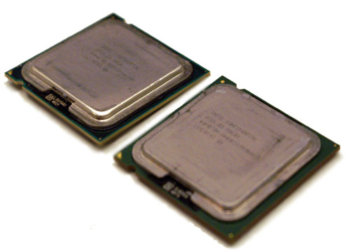
Core 2 Duo (left) vs. Pentium D (right)
What you see above appears to be no different than a Pentium D. Honestly, unless you flip it over there's no indication of what lies beneath that dull aluminum heat spreader.
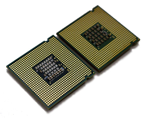
Core 2 Duo (left) vs. Pentium D (right)
But make no mistake, what you see before you is not the power hungry, poor performing, non-competitive garbage (sorry guys, it's the truth) that Intel has been shoving down our throats for the greater part of the past 5 years. No, you're instead looking at the most impressive piece of silicon the world has ever seen - and the fastest desktop processor we've ever tested. What you're looking at is Conroe and today is its birthday.
Intel's Core 2 launch lineup is fairly well rounded as you can see from the table below:
| CPU | Clock Speed | L2 Cache |
| Intel Core 2 Extreme X6800 | 2.93GHz | 4MB |
| Intel Core 2 Duo E6700 | 2.66GHz | 4MB |
| Intel Core 2 Duo E6600 | 2.40GHz | 4MB |
| Intel Core 2 Duo E6400 | 2.13GHz | 2MB |
| Intel Core 2 Duo E6300 | 1.86GHz | 2MB |
As the name implies, all Core 2 Duo CPUs are dual core as is the Core 2 Extreme. Hyper Threading is not supported on any Core 2 CPU currently on Intel's roadmaps, although a similar feature may eventually make its debut in later CPUs. All of the CPUs launching today also support Intel's Virtualization Technology (VT), run on a 1066MHz FSB and are built using 65nm transistors.
The table above features all of the Core 2 processors Intel will be releasing this year. In early next year Intel will also introduce the E4200, which will be a 1.60GHz part with only a 800MHz FSB, a 2MB cache and no VT support. The E4200 will remain a dual core part, as single core Core 2 processors won't debut until late next year. On the opposite end of the spectrum Intel will also introduce Kentsfield in Q1 next year, which will be a Core 2 Extreme branded quad core CPU from Intel.
Core 2 Extreme vs. Core 2 Duo
 Previously Intel had differentiated its "Extreme" line of processors by giving them larger caches, a faster FSB, Hyper Threading support, and/or higher clock speeds. With the Core 2 processor family, the Extreme version gets a higher clock speed (2.93GHz vs. 2.66GHz) and this time around it also gets an unlocked multiplier. Intel officially describes this feature as the following:
Core 2 Extreme is not truly "unlocked". Officially (per the BIOS Writers Guide), it is "a frequency limited processor with additional support for ratio overrides higher than the maximum Intel-tested bus-to-core ratio." Currently, that max tested ratio is 11:1 (aka 2.93G @ 1066 FSB). The min ratio is 6:1. However, do note that the Core 2 Extreme will boot at 2.93G unlike prior generation XE processors which booted to the lowest possible ratio and had to be "cranked up" to the performance ratio.
In other words, you can adjust the clock multiplier higher or lower than 11.0x, which hasn't been possible on a retail Intel chip for several years. By shipping the Core 2 Extreme unlocked, Intel has taken yet another page from AMD's Guide to Processor Success. Unfortunately for AMD, this wasn't the only page Intel took.
Manufacturing Comparison
The new Core 2 processors, regardless of L2 cache size, are made up of 291 million transistors on a 143 mm^2 die. This makes the new chips smaller and cheaper to make than Intel's Pentium D 900 series. The new Core 2 processors are also much smaller than the Athlon 64 X2s despite packing more transistors thanks to being built on a 65nm process vs. 90nm for the X2s.
| CPU | Manufacturing Process | Transistor Count | Die Size |
| AMD Athlon 64 X2 (2x512KB) | 90nm | 154M | 183 mm^2 |
| Intel Core 2 | 65nm | 291M | 143 mm^2 |
| Intel Pentium D 900 | 65nm | 376M | 162 mm^2 |
Intel's smaller die and greater number of manufacturing facilities results in greater flexibility with pricing than AMD.


202 Comments
View All Comments
invise - Friday, July 14, 2006 - link
According to page 3 "The Test", you used an Intel D975xBX motherboard (Intel 975X chipset) for the tests in the article. Yet in the picture of the Tuniq Tower on page 18 "Overclocking", there is clearly an Asus board with a gold/copper chipset heatsink, blue PCI-Express 16x slot, and alternating yellow and black DIMM slots. Which board is this? I suspect a P5WD2 or P5N32-SLI, just from looking at pictures online, but from what I can find neither of those has a gold/copper heatsink on the Northbridge.I'm curious because you got the board's FSB stable at 445 MHz, which is critical when working with a CPU with a low, locked multiplier. If any other users recognize the board please ID it.
spug1 - Friday, July 14, 2006 - link
I noticed that too Invise. Can we have some clarification as to whether you used the intel board, or the asus p5w-dh for the testing of conroe?!
cheerz, :)
JarredWalton - Friday, July 14, 2006 - link
Overclocking was done with the ASUS board. The benchmarks scores were tested on the Intel board as reported on page 3.Suraj - Friday, October 20, 2006 - link
What other parts did u change when overclocking? I'm very eager to know what exact parts u used when overclocking the e6600.Kiste - Friday, July 14, 2006 - link
Great review, as always. I have to admit though that I was hoping for a bit more with regard to i965 based mainboards.Gary Key - Friday, July 14, 2006 - link
We have a few P965 boards in house currently, however all of them are undergoing almost daily bios changes. They should be very solid from a performance viewpoint within 30 days but at this time they are still immature and any performance results shown with them are not final.
Wesley Fink - Friday, July 14, 2006 - link
You will see Conroe motherboard reviews the first of the week, and yes, there are 965 boards in the reviews.DrMrLordX - Friday, July 14, 2006 - link
Could you guys please do a mini-review of this chip? In particular, could you overclock it using a Tuniq Tower 120 or something and give us some idea of how high it will go? I've been wanting to know more about that proc since AM2 launched, but AMD has been doing a lousy job of getting them into retail channels.redpriest_ - Friday, July 14, 2006 - link
Very detailed, I loved it. But quick question: Your screenshots with cpuid have the stepping as a B1 stepping 5 Conroe - I bought a retail Conroe X6800, and it was a stepping 6 revB2 - and it "only" clocks to 3.466 ghz stably. 3.733 is unstable and 4 ghz is a no boot into Windows; so my question is - is that the stepping you used or was it just a screenshot from an older comparison?Wesley Fink - Friday, July 14, 2006 - link
Our review samples are all Stepping 5. We also have an earlier Stepping 4 unlocked E6700 that overclocks very well. We understood stepping 5 was the Retail stepping. We will clarify this with Intel later today.