ASUS M2N32-SLI & Epox MF570SLI: AM2 Wunderkinder
by Wesley Fink on June 28, 2006 5:10 AM EST- Posted in
- Motherboards
ASUS M2N32-SLI Deluxe: Basic Features & Board Layout
Current thinking in overclocking options is to provide very fine adjustments for voltages over a very wide range of control. ASUS certainly meets these expectations in the BIOS options for their new AM2 board. Memory voltage extends from 1.8V to 2.5V, but just as important is the very fine granularity of .025V increments. This provides very fine tweaking of the voltage to get the most from the memory with the least prospect for memory damage.
Similar attention to detail is evident throughout the BIOS options and feature set. Adjustable voltages are provided for just about any chip and any HT link available on the board. CPU range is 200 to 425, and each PCIe slot can have the slot speed individually controlled.
ASUS continues to set their own standards by using the ADI Soundmax Azalia HD codec instead of the more common Realtek family chips. ASUS tells us ADI has dramatically improved real-world performance of the Soundmax, and we will check this in our review on page 12.
The other unique feature of the M2N32-SLI Deluxe is the inclusion of an on-board wireless connector supporting 802.11 b/g WiFi. Not only do you get two full Gigabit LAN chips with the nForce590, you get a 3rd wireless internet connection. With the number of users building wireless home networks this is a very welcome feature for many people.
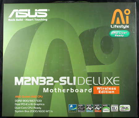
As a top-of the-line 590 board, ASUS builds on the outstanding reputation of the last-generation A8N32-SLI Deluxe. This starts with the box and logos, which are the same family design as the A8N32-SLI Deluxe.
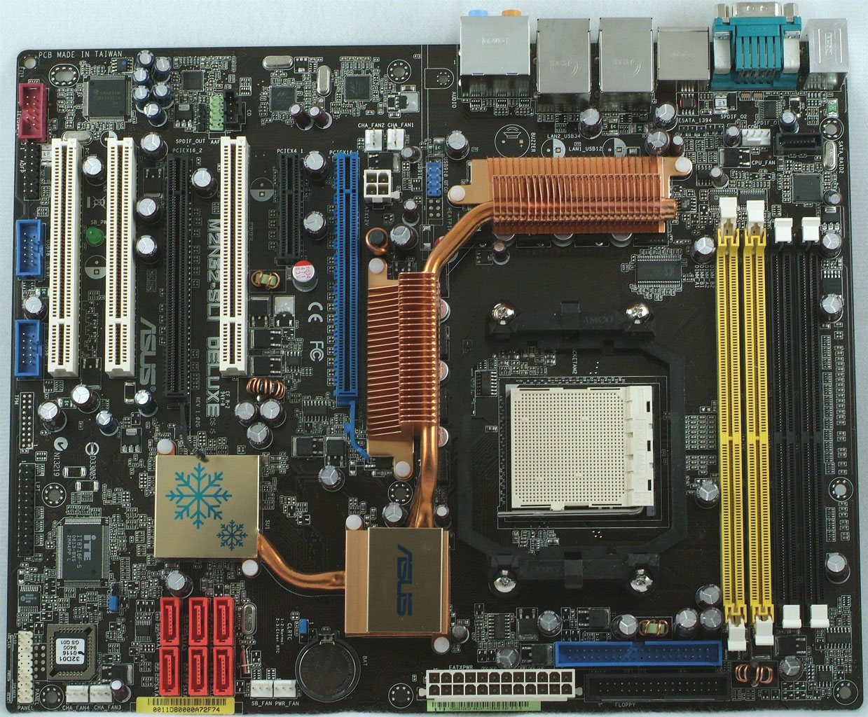
The dual X16 A8N32-SLI Deluxe was the first full 8-phase design we have tested, and ASUS continues the 8-phase design in the M2N32-SLI Deluxe. The layout is generally superb and typically ASUS, with the bulky ATX connector on the right board edge as we prefer. The 4-pin connector is in the less-desired center board location, but the copper heatsinks surrounding the CPU socket do make it a little easier to route the 4-pin cable between the heatsink and rear IO connectors to minimize interference with on-board components.
IDE/floppy connectors are in the ideal right board edge location. You will only find ONE IDE connector, however, so you will have to use SATA or USB peripherals in general. ASUS did provide the standard 6 SATA2 ports supported by 590 plus 2 more SATA2 ports supported by a Silicon Image 3132 connector.
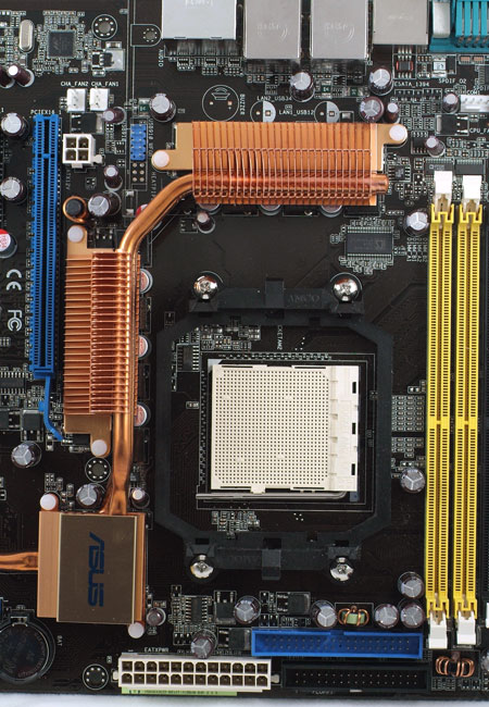
The ASUS 8-phase heatpipe and heatsink cooling system provided effective and completely passive cooling on the M2N32-SLI Deluxe. ASUS has been a proponent of passive board cooling for many years, and ASUS has managed to continue to provide passive solutions even as the chipset cooling requirements have continued to increase.
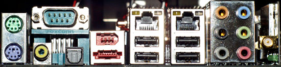
The rear IO ports combine many useful connectors. You won't find a parallel port, but you will find both optical and coaxial S/PDIF connectors along with 6 programmable mini-jacks for the High Definition sound. There is also an external SATA2 connector, an IEEE1394a Firewire port, PS/2 mouse and keyboard ports, serial port, 2 Gigabit LAN connectors, 4 USB ports, and a connector for the included antenna for the wireless LAN. Whatever you need to connect is more than likely supported on this top-of-the-line ASUS board.
| ASUS M2N32-SLI Deluxe | |
| CPU Interface | Socket AM2 |
| Chipset | NVIDIA 590 SLI MCP (ID0360) + NVIDIA 590 SLI SPP (C51-GeForce 6100/6150) |
| Bus Speeds | 200 to 425 in 1MHz Increments |
| Memory Speeds | DDR2 at Auto, 400, 533, 667, 800 |
| PCIe Speeds | 100 to 200 in 1MHz Increments (Separate Adjustments for each X16 PCIe slot) |
| AI Tuning | Manual, Auto, Standard, AI Overclock, AI N.O.S. |
| Core Voltage | Auto, 0.8V to 1.5625V in 0.0025V increments PLUS 0.2V CPU Offset (Max 1.8625V) |
| PEG Link Mode | Auto, Disabled, Normal, Fast, Faster |
| CPU Clock Multiplier | Auto, 4x-25x in 1X increments |
| DRAM Voltage | 1.8V to 2.5V in .025v increments |
| DDR2 Termination Voltage | 1.5v, 1.6v |
| 1T/2T Memory | Auto, 1T, 2T |
| AI Clock Skew | Auto, Manual |
| Manual Clock Skew | Normal, Advance or Delay 150, 300, 450, 600, 750, 900ps for EACH Channel |
| Advanced Memory Timings | 23 Options |
| DRAM Timing Control | 10 Options |
| Output Driver Control | 7 Options |
| SLI Ready Memory | Disabled, Optimal, High Performance, High Frequency |
| HyperTransport Frequency | 1000MHz (1GHz) (Stable in overclocking to 1500+ HT) |
| HyperTransport Multiplier | Auto, 1X to 5X |
| NB to SB HT | Auto, 200 to 400 in 1MHz increments |
| CPU to NB HT | Auto, 1X to 5X CPU Frequency |
| NB to SB HT | 1x to 5x NB to SB Frequency |
| SB to NB HT | 1x to 5x SB to NB Frequency |
| CPU to NB HT Width | 8up/down, 16up/down |
| NB to SB HT Width | 4up/down, 8up/down, 16up/down |
| NVIDIA GPU EX | Auto, Disabled |
| CPU to NB Voltage | Auto, 1.200v to 1.500v in 0.025v increments |
| NB to SB Voltage | Auto, 1.300v to 1.500v in 0.025v increments |
| NB Core/PCIe Voltage | Auto, 1.200v to 1.400v in 0.05v increments |
| SB Core/PCIe Voltage | Auto, 1.200v to 1.400v in 0.05v increments |
| SB Standby Voltage | 1.5v, 1.6v, 1.7v |
| AMD Live! | Disabled, Enabled |
| AMD Cool'n'Quiet | Disabled, Enabled |
| Memory Slots | Four 240-pin DDR2 DIMM Slots Dual-Channel Configuration Regular Unbuffered ECC/non ECC Memory to 16GB Total |
| Expansion Slots | 2 PCIe X16 1 PCIe X4 3 PCI Slots |
| Onboard SATA/RAID | 6 SATA2 Drives by MCP (RAID 0, 1, 1+0, 10, JBOD) PLUS 2 SATA2 Drives by Silicon Image 3132 (RAID 0, 1) (1 internal, 1 external) |
| Onboard IDE/IDE RAID | One Standard ATA133/100/66 (2 drives) |
| Onboard USB 2.0/IEEE-1394 | 10 USB 2.0 ports supported by MCP 590 2 Firewire 1394a by TI |
| Onboard LAN | DUAL PCIe Gigabit by Marvel PHY for AI Net2 PLUS WiFi 802.11b/g by Realtek RTL8187L |
| Onboard Audio | Azalia HD Audio by Soundmax ADI AD1988B 8 channel codec |
| BIOS Revision | Award 504 - June 14, 2006 |
Current thinking in overclocking options is to provide very fine adjustments for voltages over a very wide range of control. ASUS certainly meets these expectations in the BIOS options for their new AM2 board. Memory voltage extends from 1.8V to 2.5V, but just as important is the very fine granularity of .025V increments. This provides very fine tweaking of the voltage to get the most from the memory with the least prospect for memory damage.
Similar attention to detail is evident throughout the BIOS options and feature set. Adjustable voltages are provided for just about any chip and any HT link available on the board. CPU range is 200 to 425, and each PCIe slot can have the slot speed individually controlled.
ASUS continues to set their own standards by using the ADI Soundmax Azalia HD codec instead of the more common Realtek family chips. ASUS tells us ADI has dramatically improved real-world performance of the Soundmax, and we will check this in our review on page 12.
The other unique feature of the M2N32-SLI Deluxe is the inclusion of an on-board wireless connector supporting 802.11 b/g WiFi. Not only do you get two full Gigabit LAN chips with the nForce590, you get a 3rd wireless internet connection. With the number of users building wireless home networks this is a very welcome feature for many people.
As a top-of the-line 590 board, ASUS builds on the outstanding reputation of the last-generation A8N32-SLI Deluxe. This starts with the box and logos, which are the same family design as the A8N32-SLI Deluxe.
 |
| Click to enlarge |
The dual X16 A8N32-SLI Deluxe was the first full 8-phase design we have tested, and ASUS continues the 8-phase design in the M2N32-SLI Deluxe. The layout is generally superb and typically ASUS, with the bulky ATX connector on the right board edge as we prefer. The 4-pin connector is in the less-desired center board location, but the copper heatsinks surrounding the CPU socket do make it a little easier to route the 4-pin cable between the heatsink and rear IO connectors to minimize interference with on-board components.
IDE/floppy connectors are in the ideal right board edge location. You will only find ONE IDE connector, however, so you will have to use SATA or USB peripherals in general. ASUS did provide the standard 6 SATA2 ports supported by 590 plus 2 more SATA2 ports supported by a Silicon Image 3132 connector.
The ASUS 8-phase heatpipe and heatsink cooling system provided effective and completely passive cooling on the M2N32-SLI Deluxe. ASUS has been a proponent of passive board cooling for many years, and ASUS has managed to continue to provide passive solutions even as the chipset cooling requirements have continued to increase.
The rear IO ports combine many useful connectors. You won't find a parallel port, but you will find both optical and coaxial S/PDIF connectors along with 6 programmable mini-jacks for the High Definition sound. There is also an external SATA2 connector, an IEEE1394a Firewire port, PS/2 mouse and keyboard ports, serial port, 2 Gigabit LAN connectors, 4 USB ports, and a connector for the included antenna for the wireless LAN. Whatever you need to connect is more than likely supported on this top-of-the-line ASUS board.


23 Comments
View All Comments
Missing Ghost - Wednesday, June 28, 2006 - link
yep the choice of I/O ports on the back panel is pretty poorLarso - Wednesday, June 28, 2006 - link
Perhaps someone should clarify this for me. I have been noticing how there is a growing interest in how the motherboard makers have done the power conversion for the CPU. Why has this become an issue to investigate?I don't think there was a similar focus on the power converters for the netburst chips, which I believe soaked a lot more juice than these AMD chips. I believe they managed to deliver stable power to the netbursts without needing an 8 phase converter cooled by heatpipes??
I'm fearing that the motherboard producers will start to create extravagant and foolishly designed converters to please the reviewers. I believe there is no good reason to go for an 8 phase design, when a 4 phase would do the job, considering the money that can be spend on each phase. And that ASUS need to cool the converter by heatpipe seems to indicate that the convertion have a bad effeciency, is this really a step forward?
I really enjoy reading more about the technical solutions on the motherboards, but it just seems to me that the power converter should be less of an issue now, than with the power hungry netburts?
Operandi - Friday, June 30, 2006 - link
A 8 phase design is more efficient then a 4 phase, not less.Missing Ghost - Wednesday, June 28, 2006 - link
It seems to me that the heatpipes are more for cooling the chipset in fact.erwos - Wednesday, June 28, 2006 - link
What WiFi chipset does it use? "It has WiFi" is not terribly precise.-Erwos
Wesley Fink - Wednesday, June 28, 2006 - link
The WiFi chip used on the Asus WiFi module is Realtek RTL8187L. The Features have been updated to reflect this.Wesley Fink - Wednesday, June 28, 2006 - link
Asus refers to the Wi-Fi in specifications as "WiFi Home USB wireless module supporting IEE 802.11 b/g". There is no mention at all of the supporting chip. The module is attached to the motherboard and the chip is loacated behind heatpipes. We can't read the model number, but the logo is clearly Realtek.highlnder69 - Wednesday, June 28, 2006 - link
On page 8 under Half Life 2 - SLI Gaming Performance, I think that the Asus Single/SLI results are labeled incorrectly. It's currently showing the Single card configuration with the highest FPS results and the SLI with the lowest.Wesley Fink - Wednesday, June 28, 2006 - link
You are correct, the labels were reversed. They are now corrected.DigitalFreak - Wednesday, June 28, 2006 - link
Someone needs to teach the idiots at Asus about how to design the proper motherboard layout. With an SLI setup with dual width cards, there's no PCI-E slots available.