K8L Architecture
At the outset, we hoped we'd have a very large section on AMD's new architecture. After our whirlwind of a three hour briefing, we aren't that much further along on the K8L architecture front than we were before. We've had some things confirmed by a few slides, but AMD didn't spend much time on these details. Over the next few days we will be sitting down with AMD and gathering as much detailed information about K8L as we can, but for now we can offer an overview of what we already know and have gathered from the slides we've seen.
The first K8L chips will be fabbed on a 65nm SOI process jointly developed by IBM and AMD, and manufactured at AMD facilities in Dresden. AMD has implemented a more modular approach to designing their next gen CPUs this time around in order to more easily meet the demands of a market craving ever increasing support for multicore technology. While CPUs are traditionally very hand tuned and designed on a low level, it appears AMD has taken an extremely object oriented approach to CPU design. The interfaces between different parts of the CPU are very strongly defined and it is possible for AMD to mix and match components as necessary.
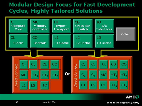
This type of approach makes a lot of sense in today's world. Designing processors without the need to reengineer the entire CPU from the ground up in order to add another compute core, HT link or (maybe) another memory controller is a stroke of brilliance. Dual and quad core systems don't need 2 or four of everything, but needs do change depending on the application targeted by the hardware. Hopefully AMD will use this technology to enable the delivery of changing CPU configurations much the same way we see clock speeds and cache sizes change over time today.
On a very slightly lower level architecture side, we have a slide showing the overview of AMD's next server class processor with 4 cores based on K8L. Features include a shared L3 cache, "enhanced IPC" cores, OoO (Out of Order) loads, wider data paths, HT-3 (the third version of HyperTransport), and support for DDR2 (and DDR3 or FBDIMMS in the future). Details on some of these enhancements were way too light, especially on the IPC (Instructions Per Clock) front.
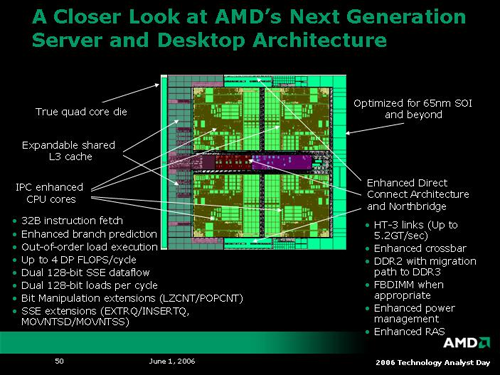
Cache enhancements include the capability to support 2x128-bit loads per cycle from the 64k L1 cache (which is half the size of the K8 L1 cache), and a shared L3 cache which will scale up from its introduction at 2MB. The shared L3 cache will help with features like node interleaving on multiprocessor systems as well as multithreaded apps which make use of shared data. We are still waiting for more detailed data on the cache architecture. It isn't clear whether the caches are all exclusive, and we would like to know more about associativity as well.
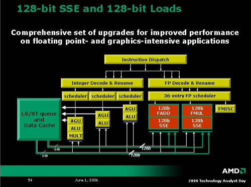
At a lower level, we have a block diagram of the compute core for K8L CPUs. Again, this diagram is a bit oversimplified, but we can see a few key features of the architecture. On the FP side, the CPU is able to handle 2x128-bit floating point or SSE operations per clock. While this isn't quite as flexible as Intel's Core with its 3 SSE units, AMD's K8L will be able to handle 4 double precision floating point operations per clock. . (Current K8 chips can only do 1x128/2x64-bit SSE instructions per clock.)
As with K8, K8L will have 3 ALUs (arithmetic logic units) and 3 AGUs (address generation units). Combined with cache enhancements and the new ability to reorder loads, K8L has a shot at outpacing Core in integer performance. Of course, we do still need more detail in this area to understand fully what's going on. No doubt, if AMD is claiming the ability to reorder loads, they can absolutely move loads ahead of loads (as this is the easiest case to handle). Where things get interesting is in the ability to move loads ahead of stores. Intel's Core architecture features some very interesting prediction technology in determining whether or not to move a load before a store. We haven't received an answer from AMD on whether they will tackle moving loads ahead of stores at all, let alone how they will handle memory disambiguation and/or prediction. In the past, we've seen a kind of "simpler is better" approach from AMD, so it will be interesting to see which direction K8L has taken.
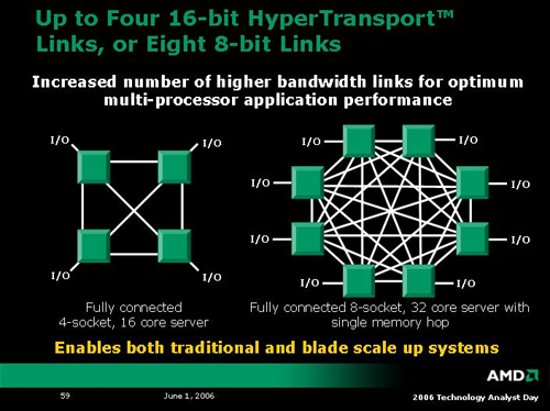
When it comes to processor interconnect technology, AMD has led Intel since the introduction of the Opteron. With K8L comes a very interesting enhancement to the interconnect architecture: each of the four 16-bit HyperTransport links can be split into two 8-bit HyperTransport links. Apparently, each of the resulting eight 8-bit HT links will be coherent and will allow a direct connection to another processor. In large systems, this means direct access from one core to seven others plus I/O, resulting in the possibility of fully connected 8-way systems. In a quad core world, that would be 32 cores on one platform. AMD also indicates that these HT connections can be used to easily scale blade implementations as well.
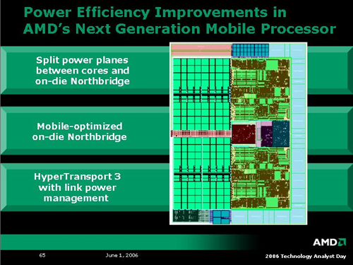
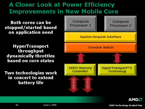
AMD mobile processors will also benefit from enhancements to HyperTransport with link power management. Not only will the new dual core 65nm K8L Turion processors be able to throttle cores independently, but even the HT links can be powered down when not in use. These enhancements will go a long way towards expanding AMD's mobile capabilities, especially if the K8L architecture can deliver better performance per Watt than the K8 before it. Compared to NetBurst architectures, K8 may as well have been an icebox, but that all changed with the introduction of Banias, Dothan, Yonah and now Core technology. Intel is bringing the fight to AMD, and K8L will need to deliver on the power front in order to remain competitive. The only market segment that really throws power to the wind is the extreme enthusiast (to which AMD's 4x4 initiative will certainly cater), but volume business will require an eye to the efficient.
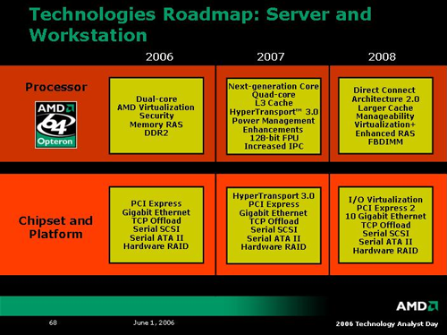
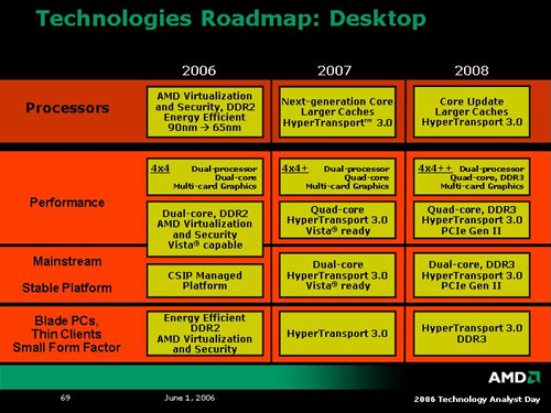
To round out what we learned about K8L architecture, here are the roadmap slides of technology AMD plans to roll out over the next three years.
At the outset, we hoped we'd have a very large section on AMD's new architecture. After our whirlwind of a three hour briefing, we aren't that much further along on the K8L architecture front than we were before. We've had some things confirmed by a few slides, but AMD didn't spend much time on these details. Over the next few days we will be sitting down with AMD and gathering as much detailed information about K8L as we can, but for now we can offer an overview of what we already know and have gathered from the slides we've seen.
The first K8L chips will be fabbed on a 65nm SOI process jointly developed by IBM and AMD, and manufactured at AMD facilities in Dresden. AMD has implemented a more modular approach to designing their next gen CPUs this time around in order to more easily meet the demands of a market craving ever increasing support for multicore technology. While CPUs are traditionally very hand tuned and designed on a low level, it appears AMD has taken an extremely object oriented approach to CPU design. The interfaces between different parts of the CPU are very strongly defined and it is possible for AMD to mix and match components as necessary.
This type of approach makes a lot of sense in today's world. Designing processors without the need to reengineer the entire CPU from the ground up in order to add another compute core, HT link or (maybe) another memory controller is a stroke of brilliance. Dual and quad core systems don't need 2 or four of everything, but needs do change depending on the application targeted by the hardware. Hopefully AMD will use this technology to enable the delivery of changing CPU configurations much the same way we see clock speeds and cache sizes change over time today.
On a very slightly lower level architecture side, we have a slide showing the overview of AMD's next server class processor with 4 cores based on K8L. Features include a shared L3 cache, "enhanced IPC" cores, OoO (Out of Order) loads, wider data paths, HT-3 (the third version of HyperTransport), and support for DDR2 (and DDR3 or FBDIMMS in the future). Details on some of these enhancements were way too light, especially on the IPC (Instructions Per Clock) front.
Cache enhancements include the capability to support 2x128-bit loads per cycle from the 64k L1 cache (which is half the size of the K8 L1 cache), and a shared L3 cache which will scale up from its introduction at 2MB. The shared L3 cache will help with features like node interleaving on multiprocessor systems as well as multithreaded apps which make use of shared data. We are still waiting for more detailed data on the cache architecture. It isn't clear whether the caches are all exclusive, and we would like to know more about associativity as well.
At a lower level, we have a block diagram of the compute core for K8L CPUs. Again, this diagram is a bit oversimplified, but we can see a few key features of the architecture. On the FP side, the CPU is able to handle 2x128-bit floating point or SSE operations per clock. While this isn't quite as flexible as Intel's Core with its 3 SSE units, AMD's K8L will be able to handle 4 double precision floating point operations per clock. . (Current K8 chips can only do 1x128/2x64-bit SSE instructions per clock.)
As with K8, K8L will have 3 ALUs (arithmetic logic units) and 3 AGUs (address generation units). Combined with cache enhancements and the new ability to reorder loads, K8L has a shot at outpacing Core in integer performance. Of course, we do still need more detail in this area to understand fully what's going on. No doubt, if AMD is claiming the ability to reorder loads, they can absolutely move loads ahead of loads (as this is the easiest case to handle). Where things get interesting is in the ability to move loads ahead of stores. Intel's Core architecture features some very interesting prediction technology in determining whether or not to move a load before a store. We haven't received an answer from AMD on whether they will tackle moving loads ahead of stores at all, let alone how they will handle memory disambiguation and/or prediction. In the past, we've seen a kind of "simpler is better" approach from AMD, so it will be interesting to see which direction K8L has taken.
When it comes to processor interconnect technology, AMD has led Intel since the introduction of the Opteron. With K8L comes a very interesting enhancement to the interconnect architecture: each of the four 16-bit HyperTransport links can be split into two 8-bit HyperTransport links. Apparently, each of the resulting eight 8-bit HT links will be coherent and will allow a direct connection to another processor. In large systems, this means direct access from one core to seven others plus I/O, resulting in the possibility of fully connected 8-way systems. In a quad core world, that would be 32 cores on one platform. AMD also indicates that these HT connections can be used to easily scale blade implementations as well.
AMD mobile processors will also benefit from enhancements to HyperTransport with link power management. Not only will the new dual core 65nm K8L Turion processors be able to throttle cores independently, but even the HT links can be powered down when not in use. These enhancements will go a long way towards expanding AMD's mobile capabilities, especially if the K8L architecture can deliver better performance per Watt than the K8 before it. Compared to NetBurst architectures, K8 may as well have been an icebox, but that all changed with the introduction of Banias, Dothan, Yonah and now Core technology. Intel is bringing the fight to AMD, and K8L will need to deliver on the power front in order to remain competitive. The only market segment that really throws power to the wind is the extreme enthusiast (to which AMD's 4x4 initiative will certainly cater), but volume business will require an eye to the efficient.
To round out what we learned about K8L architecture, here are the roadmap slides of technology AMD plans to roll out over the next three years.


40 Comments
View All Comments
HurleyBird - Friday, June 2, 2006 - link
HyperTransport was created by AMD. The consortium was created afterwards to manage the standard.
od4hs - Friday, June 2, 2006 - link
AMD began developing the HyperTransport™ I/O link architecture in 1997.Pre-Consortium Versions of the Specification
AMD has released these two pre-consortium documents which define two revisions of "LDT" (Lightning Data Transfer) as HT was known before the HT Consortium was formed.
http://www.hypertransport.org/tech/tech_specs.cfm">http://www.hypertransport.org/tech/tech_specs.cfm
[2001]
AMD has disclosed HyperTransport technology specifications under non-disclosure
agreement (NDA) to over 170 companies interested in building products that incorporate
this technology.
Multiple partners have signed the license agreement for HyperTransport technology,
including, among many others:
Sun Microsystems Cisco Systems Broadcom
Texas Instruments NVIDIA Acer Labs
Hewlett-Packard Schlumberger Stargen
PLX Technology Mellanox FuturePlus
API Networks Altera LSI Logic
PMC-Sierra Pericom Transmeta
AMD is releasing the specifications to an industry-supported non-profit trade association in the fall of 2001.
The HyperTransport Consortium will manage and refine the specifications, and
promote the adoption and deployment of HyperTransport technology. It is also expected
to consist initially of a Technical Working Group and a Marketing Working Group.
Subordinate task forces will do the work of the consortium. Anticipated technical task
forces include:
Protocol Task Force
Connectivity Task Force
Graphics Task Force
Technology Task Force
Power Management Task Force
Information on joining the HyperTransport Technology Consortium can be found at
this website: http://www.hypertransport.org">http://www.hypertransport.org
http://www.amd.com/us-en/assets/content_type/white...">HyperTransport Technology I/O Link (white paper), PDF
San Jose, Calif., July 24, 2001 -- A coalition of high-tech industry leaders today announced the formation of the HyperTransport™ Technology Consortium, a nonprofit corporation that supports the future development and adoption of AMD's HyperTransport I/O Link specification.
[...] More than 180 companies throughout the computer and communications industries have been engaged with AMD in working with the HyperTransport technology
http://www.hypertransport.org/consortium/cons_pres...">hypertransport.org press release
peternelson - Friday, June 2, 2006 - link
HT 1,2,and 3 are published standards.
Direct Connect Architecture (DCA 1.0 and 2.0 are published standards).
HTX is a published standard.
Some questions for you to ask the AMD engineers:
I'm still interested to obtain pinouts of AM2 and F1207 sockets to establish how many HT links they can support.
From 4x4 it looks like AM2 *MIGHT* support TWO HT links (one to other processor, one to the tunnel chip.
I note 4x4 is slated for 2006 launch.
Hope to see those boards real soon ;-) I assume you can populate one socket and put the other proc in there later when you have more money ;-)
I would like to see HTX appear on some 4x4 or AM2 boards but doubt it will happen.
However, on the "acceleration technology" I would like 4x4 to support the so-called "socketfiller" type where you drop in a xilinx fpga onto the socket. That would give a cheap 1cpu + 1fpga system. Hopefully acceleration is not precluded just cos its not opteron and not 1207.
Now thinking of opterons, I want to know the pinout of socket F. I want to count the HT link support built in to the socket. If its only 3 HT links that would force a socket change to do 4 links.
What news on possible future socket change requirements? eg for ddr3 and HT3 speed?
Can the Nvidia chipset for opteron be built onto an AM2 board?
I would encourage many board makers to add HTX to their opteron boards (easy and worthwhile) because eg one example is the pathscale HTX cluster interconnect cards.
I am interested in AMD terms for licensing of any proprietary tech for their cache coherency, or DCA2, any white papers on it or reference designs.
Is the 4x4+ in 2007 only K8 quadcore or is it K8L quadcore?
Will K8L be supported on AM2 socket?
Please encourage AMD to publish web datasheets on AM2 as exist for their old sockets.
saratoga - Friday, June 2, 2006 - link
I think any HT compliant chipset can be used with any HT compliant part. Thats why Apple can use AMD's PCI-X bridge designed for Opteron processors on their older G5 systems. The chipset supports HT, thats all you need.
I don't know if that changes with the new HT standards though.
peternelson - Friday, June 2, 2006 - link
*IF* an am2 socket can indeed support TWO HT links, then the SECOND processor could use its spare link to connect to yet another I/O interface chip/chipset.This would give opportunity for innovative 4x4 boards to add additional I/O, more pcie links, or an HTX slot.
Please can we verify:
How many links are available on AM2, and howmany links are available on FX62, and how many links are available on lower AM2 chips. I suspect the lower ones only have one HT link which would make them unsuitable for 4x4 operation. Please confirm.
Jellodyne - Friday, June 2, 2006 - link
There's a few of ways 4x4 could work with only the one HTT link in the socket.1. AMD could enable a second chip-to-chip HTT link using pins/lands on top of the cpu, or some sort of edge connector, with a pcb which bridges the two.
or
2. AMD could be splitting the HTT link into 2 8-bit links. One to the chipset, one to the 2nd processor. Heck, if the chipset is smart enough the leftover 8 bit link could go back to the chipset, resulting in the equivalent bandwidth between chipset and processors as a 'standard' dual opteron rig, just less between the processors. For desktops, 8 bit is probably enough.
and of course if you're talking custom chipset, that leaves
3. The chipset has dual CHT links, one to each processor, and acts like a traditional dual FSB chipset.
I'd say #2 is pretty likely.
Squidward - Friday, June 2, 2006 - link
Whoever designs those slides should be fired or at least taught some color coordination. They hurt my eyes.Now dual slot - dual core mobos sound tasty but the price would be astronimical to configure a killer system. (looks at outdated Athlon 2500+ and sighs)
Calin - Monday, June 5, 2006 - link
(looks at outdated Duron 600 and cries)LoneWolf15 - Monday, June 5, 2006 - link
Time to draw the L1 bridges shut and clock your way up, my friend.My Duron 600 made 1GHz when cooled right --it was cooler at 7.5 x 133 than at 10.0 x 100.
And if you fry the chip, well...a used Duron, Thunderbird, or Palomino core is relatively inexpensive these days...
Frallan - Monday, June 5, 2006 - link
Well at least U guys have saved some money on the way of beeing outdated...*looks at outdated 3500+, 6800Gt@Ultra, 2*1Gb Ram and empty wallet and howls with pain*
/F