Introduction & Manufacturing
AMD held its spring Analyst Day on Thursday, and we were able to sit down and enjoy the webcast. While we fully expected to learn about AMD's next CPU architecture, K8L, we were pleasantly surprised to find a few unexpected extras. The event covered a huge swath of the computing industry in a manner that went just deep enough to leave us screaming for more. Unfortunately, we don't have all the answers we wanted today, but we do have some good ideas about what we'll be seeing in the near future about AMD's upcoming technology.
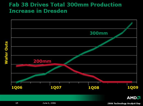
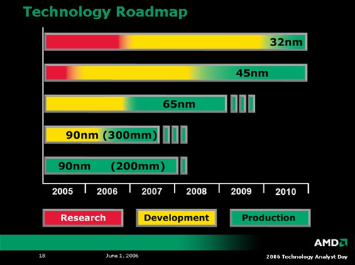
As could be expected, the day started off with an overview of AMD's fabrication strategies. In the near term, AMD is transitioning from 200mm wafers for its 90nm SOI process to 300mm wafers. This will help serve to get AMD up to speed with 300mm wafer before volume production of 65nm devices begins. As 200mm wafer production is phased out, 65nm processes will be ramping into full swing. AMD plans on an aggressive schedule for transitioning to the smaller process technology, and an even more aggressive schedule for pushing out 45nm technology after this product cycle. As of now, AMD plans to introduce production 45nm silicon only 18 months after 65nm hardware hits the market.
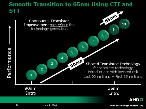
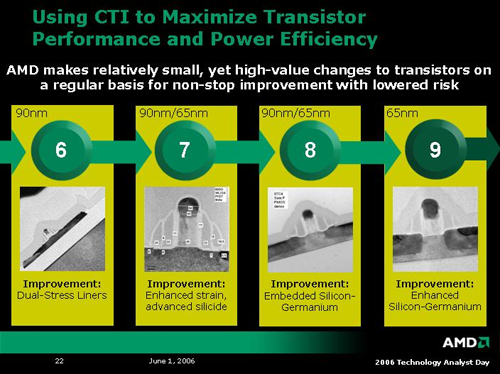
In moving to 65nm, AMD has adopted a strategy of constant improvement of its current transistor technology to ensure a smooth transition. The last generation 90nm parts will overlap the first generation 65nm parts, as many of the key features of their structures will be shared. AMD calls this Shared Transistor Technology and Continuous Transistor Improvement. As small improvements are made over the entire life cycle of a process, the final transition from one type of process to another is made much easier.
After AMD showed off a bunch of slides about how their fab is better than your fab, they started to touch on a few topics that really get our groove on: platform architecture. AMD introduced three new platform initiatives, and talked a little bit about their K8L architecture. First we'll talk about the direction AMD is moving with their platform technology.
AMD held its spring Analyst Day on Thursday, and we were able to sit down and enjoy the webcast. While we fully expected to learn about AMD's next CPU architecture, K8L, we were pleasantly surprised to find a few unexpected extras. The event covered a huge swath of the computing industry in a manner that went just deep enough to leave us screaming for more. Unfortunately, we don't have all the answers we wanted today, but we do have some good ideas about what we'll be seeing in the near future about AMD's upcoming technology.
As could be expected, the day started off with an overview of AMD's fabrication strategies. In the near term, AMD is transitioning from 200mm wafers for its 90nm SOI process to 300mm wafers. This will help serve to get AMD up to speed with 300mm wafer before volume production of 65nm devices begins. As 200mm wafer production is phased out, 65nm processes will be ramping into full swing. AMD plans on an aggressive schedule for transitioning to the smaller process technology, and an even more aggressive schedule for pushing out 45nm technology after this product cycle. As of now, AMD plans to introduce production 45nm silicon only 18 months after 65nm hardware hits the market.
In moving to 65nm, AMD has adopted a strategy of constant improvement of its current transistor technology to ensure a smooth transition. The last generation 90nm parts will overlap the first generation 65nm parts, as many of the key features of their structures will be shared. AMD calls this Shared Transistor Technology and Continuous Transistor Improvement. As small improvements are made over the entire life cycle of a process, the final transition from one type of process to another is made much easier.
After AMD showed off a bunch of slides about how their fab is better than your fab, they started to touch on a few topics that really get our groove on: platform architecture. AMD introduced three new platform initiatives, and talked a little bit about their K8L architecture. First we'll talk about the direction AMD is moving with their platform technology.


40 Comments
View All Comments
HurleyBird - Friday, June 2, 2006 - link
HyperTransport was created by AMD. The consortium was created afterwards to manage the standard.
od4hs - Friday, June 2, 2006 - link
AMD began developing the HyperTransport™ I/O link architecture in 1997.Pre-Consortium Versions of the Specification
AMD has released these two pre-consortium documents which define two revisions of "LDT" (Lightning Data Transfer) as HT was known before the HT Consortium was formed.
http://www.hypertransport.org/tech/tech_specs.cfm">http://www.hypertransport.org/tech/tech_specs.cfm
[2001]
AMD has disclosed HyperTransport technology specifications under non-disclosure
agreement (NDA) to over 170 companies interested in building products that incorporate
this technology.
Multiple partners have signed the license agreement for HyperTransport technology,
including, among many others:
Sun Microsystems Cisco Systems Broadcom
Texas Instruments NVIDIA Acer Labs
Hewlett-Packard Schlumberger Stargen
PLX Technology Mellanox FuturePlus
API Networks Altera LSI Logic
PMC-Sierra Pericom Transmeta
AMD is releasing the specifications to an industry-supported non-profit trade association in the fall of 2001.
The HyperTransport Consortium will manage and refine the specifications, and
promote the adoption and deployment of HyperTransport technology. It is also expected
to consist initially of a Technical Working Group and a Marketing Working Group.
Subordinate task forces will do the work of the consortium. Anticipated technical task
forces include:
Protocol Task Force
Connectivity Task Force
Graphics Task Force
Technology Task Force
Power Management Task Force
Information on joining the HyperTransport Technology Consortium can be found at
this website: http://www.hypertransport.org">http://www.hypertransport.org
http://www.amd.com/us-en/assets/content_type/white...">HyperTransport Technology I/O Link (white paper), PDF
San Jose, Calif., July 24, 2001 -- A coalition of high-tech industry leaders today announced the formation of the HyperTransport™ Technology Consortium, a nonprofit corporation that supports the future development and adoption of AMD's HyperTransport I/O Link specification.
[...] More than 180 companies throughout the computer and communications industries have been engaged with AMD in working with the HyperTransport technology
http://www.hypertransport.org/consortium/cons_pres...">hypertransport.org press release
peternelson - Friday, June 2, 2006 - link
HT 1,2,and 3 are published standards.
Direct Connect Architecture (DCA 1.0 and 2.0 are published standards).
HTX is a published standard.
Some questions for you to ask the AMD engineers:
I'm still interested to obtain pinouts of AM2 and F1207 sockets to establish how many HT links they can support.
From 4x4 it looks like AM2 *MIGHT* support TWO HT links (one to other processor, one to the tunnel chip.
I note 4x4 is slated for 2006 launch.
Hope to see those boards real soon ;-) I assume you can populate one socket and put the other proc in there later when you have more money ;-)
I would like to see HTX appear on some 4x4 or AM2 boards but doubt it will happen.
However, on the "acceleration technology" I would like 4x4 to support the so-called "socketfiller" type where you drop in a xilinx fpga onto the socket. That would give a cheap 1cpu + 1fpga system. Hopefully acceleration is not precluded just cos its not opteron and not 1207.
Now thinking of opterons, I want to know the pinout of socket F. I want to count the HT link support built in to the socket. If its only 3 HT links that would force a socket change to do 4 links.
What news on possible future socket change requirements? eg for ddr3 and HT3 speed?
Can the Nvidia chipset for opteron be built onto an AM2 board?
I would encourage many board makers to add HTX to their opteron boards (easy and worthwhile) because eg one example is the pathscale HTX cluster interconnect cards.
I am interested in AMD terms for licensing of any proprietary tech for their cache coherency, or DCA2, any white papers on it or reference designs.
Is the 4x4+ in 2007 only K8 quadcore or is it K8L quadcore?
Will K8L be supported on AM2 socket?
Please encourage AMD to publish web datasheets on AM2 as exist for their old sockets.
saratoga - Friday, June 2, 2006 - link
I think any HT compliant chipset can be used with any HT compliant part. Thats why Apple can use AMD's PCI-X bridge designed for Opteron processors on their older G5 systems. The chipset supports HT, thats all you need.
I don't know if that changes with the new HT standards though.
peternelson - Friday, June 2, 2006 - link
*IF* an am2 socket can indeed support TWO HT links, then the SECOND processor could use its spare link to connect to yet another I/O interface chip/chipset.This would give opportunity for innovative 4x4 boards to add additional I/O, more pcie links, or an HTX slot.
Please can we verify:
How many links are available on AM2, and howmany links are available on FX62, and how many links are available on lower AM2 chips. I suspect the lower ones only have one HT link which would make them unsuitable for 4x4 operation. Please confirm.
Jellodyne - Friday, June 2, 2006 - link
There's a few of ways 4x4 could work with only the one HTT link in the socket.1. AMD could enable a second chip-to-chip HTT link using pins/lands on top of the cpu, or some sort of edge connector, with a pcb which bridges the two.
or
2. AMD could be splitting the HTT link into 2 8-bit links. One to the chipset, one to the 2nd processor. Heck, if the chipset is smart enough the leftover 8 bit link could go back to the chipset, resulting in the equivalent bandwidth between chipset and processors as a 'standard' dual opteron rig, just less between the processors. For desktops, 8 bit is probably enough.
and of course if you're talking custom chipset, that leaves
3. The chipset has dual CHT links, one to each processor, and acts like a traditional dual FSB chipset.
I'd say #2 is pretty likely.
Squidward - Friday, June 2, 2006 - link
Whoever designs those slides should be fired or at least taught some color coordination. They hurt my eyes.Now dual slot - dual core mobos sound tasty but the price would be astronimical to configure a killer system. (looks at outdated Athlon 2500+ and sighs)
Calin - Monday, June 5, 2006 - link
(looks at outdated Duron 600 and cries)LoneWolf15 - Monday, June 5, 2006 - link
Time to draw the L1 bridges shut and clock your way up, my friend.My Duron 600 made 1GHz when cooled right --it was cooler at 7.5 x 133 than at 10.0 x 100.
And if you fry the chip, well...a used Duron, Thunderbird, or Palomino core is relatively inexpensive these days...
Frallan - Monday, June 5, 2006 - link
Well at least U guys have saved some money on the way of beeing outdated...*looks at outdated 3500+, 6800Gt@Ultra, 2*1Gb Ram and empty wallet and howls with pain*
/F