K8L Architecture
At the outset, we hoped we'd have a very large section on AMD's new architecture. After our whirlwind of a three hour briefing, we aren't that much further along on the K8L architecture front than we were before. We've had some things confirmed by a few slides, but AMD didn't spend much time on these details. Over the next few days we will be sitting down with AMD and gathering as much detailed information about K8L as we can, but for now we can offer an overview of what we already know and have gathered from the slides we've seen.
The first K8L chips will be fabbed on a 65nm SOI process jointly developed by IBM and AMD, and manufactured at AMD facilities in Dresden. AMD has implemented a more modular approach to designing their next gen CPUs this time around in order to more easily meet the demands of a market craving ever increasing support for multicore technology. While CPUs are traditionally very hand tuned and designed on a low level, it appears AMD has taken an extremely object oriented approach to CPU design. The interfaces between different parts of the CPU are very strongly defined and it is possible for AMD to mix and match components as necessary.
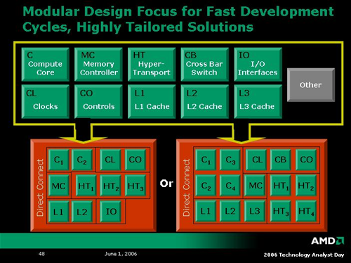
This type of approach makes a lot of sense in today's world. Designing processors without the need to reengineer the entire CPU from the ground up in order to add another compute core, HT link or (maybe) another memory controller is a stroke of brilliance. Dual and quad core systems don't need 2 or four of everything, but needs do change depending on the application targeted by the hardware. Hopefully AMD will use this technology to enable the delivery of changing CPU configurations much the same way we see clock speeds and cache sizes change over time today.
On a very slightly lower level architecture side, we have a slide showing the overview of AMD's next server class processor with 4 cores based on K8L. Features include a shared L3 cache, "enhanced IPC" cores, OoO (Out of Order) loads, wider data paths, HT-3 (the third version of HyperTransport), and support for DDR2 (and DDR3 or FBDIMMS in the future). Details on some of these enhancements were way too light, especially on the IPC (Instructions Per Clock) front.
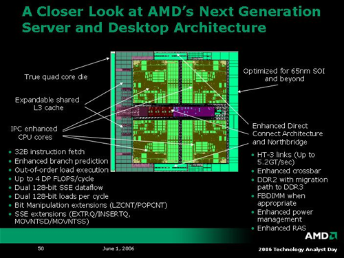
Cache enhancements include the capability to support 2x128-bit loads per cycle from the 64k L1 cache (which is half the size of the K8 L1 cache), and a shared L3 cache which will scale up from its introduction at 2MB. The shared L3 cache will help with features like node interleaving on multiprocessor systems as well as multithreaded apps which make use of shared data. We are still waiting for more detailed data on the cache architecture. It isn't clear whether the caches are all exclusive, and we would like to know more about associativity as well.
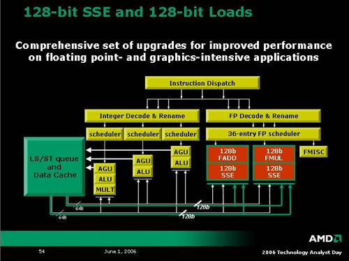
At a lower level, we have a block diagram of the compute core for K8L CPUs. Again, this diagram is a bit oversimplified, but we can see a few key features of the architecture. On the FP side, the CPU is able to handle 2x128-bit floating point or SSE operations per clock. While this isn't quite as flexible as Intel's Core with its 3 SSE units, AMD's K8L will be able to handle 4 double precision floating point operations per clock. . (Current K8 chips can only do 1x128/2x64-bit SSE instructions per clock.)
As with K8, K8L will have 3 ALUs (arithmetic logic units) and 3 AGUs (address generation units). Combined with cache enhancements and the new ability to reorder loads, K8L has a shot at outpacing Core in integer performance. Of course, we do still need more detail in this area to understand fully what's going on. No doubt, if AMD is claiming the ability to reorder loads, they can absolutely move loads ahead of loads (as this is the easiest case to handle). Where things get interesting is in the ability to move loads ahead of stores. Intel's Core architecture features some very interesting prediction technology in determining whether or not to move a load before a store. We haven't received an answer from AMD on whether they will tackle moving loads ahead of stores at all, let alone how they will handle memory disambiguation and/or prediction. In the past, we've seen a kind of "simpler is better" approach from AMD, so it will be interesting to see which direction K8L has taken.
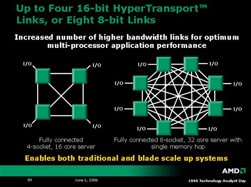
When it comes to processor interconnect technology, AMD has led Intel since the introduction of the Opteron. With K8L comes a very interesting enhancement to the interconnect architecture: each of the four 16-bit HyperTransport links can be split into two 8-bit HyperTransport links. Apparently, each of the resulting eight 8-bit HT links will be coherent and will allow a direct connection to another processor. In large systems, this means direct access from one core to seven others plus I/O, resulting in the possibility of fully connected 8-way systems. In a quad core world, that would be 32 cores on one platform. AMD also indicates that these HT connections can be used to easily scale blade implementations as well.
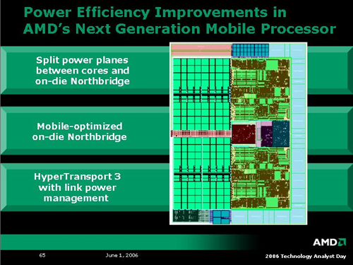
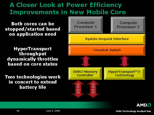
AMD mobile processors will also benefit from enhancements to HyperTransport with link power management. Not only will the new dual core 65nm K8L Turion processors be able to throttle cores independently, but even the HT links can be powered down when not in use. These enhancements will go a long way towards expanding AMD's mobile capabilities, especially if the K8L architecture can deliver better performance per Watt than the K8 before it. Compared to NetBurst architectures, K8 may as well have been an icebox, but that all changed with the introduction of Banias, Dothan, Yonah and now Core technology. Intel is bringing the fight to AMD, and K8L will need to deliver on the power front in order to remain competitive. The only market segment that really throws power to the wind is the extreme enthusiast (to which AMD's 4x4 initiative will certainly cater), but volume business will require an eye to the efficient.
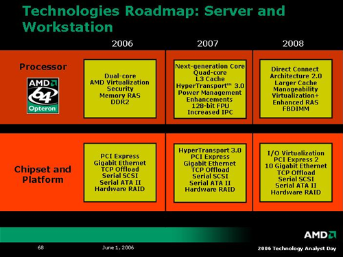
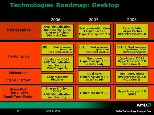
To round out what we learned about K8L architecture, here are the roadmap slides of technology AMD plans to roll out over the next three years.
At the outset, we hoped we'd have a very large section on AMD's new architecture. After our whirlwind of a three hour briefing, we aren't that much further along on the K8L architecture front than we were before. We've had some things confirmed by a few slides, but AMD didn't spend much time on these details. Over the next few days we will be sitting down with AMD and gathering as much detailed information about K8L as we can, but for now we can offer an overview of what we already know and have gathered from the slides we've seen.
The first K8L chips will be fabbed on a 65nm SOI process jointly developed by IBM and AMD, and manufactured at AMD facilities in Dresden. AMD has implemented a more modular approach to designing their next gen CPUs this time around in order to more easily meet the demands of a market craving ever increasing support for multicore technology. While CPUs are traditionally very hand tuned and designed on a low level, it appears AMD has taken an extremely object oriented approach to CPU design. The interfaces between different parts of the CPU are very strongly defined and it is possible for AMD to mix and match components as necessary.
This type of approach makes a lot of sense in today's world. Designing processors without the need to reengineer the entire CPU from the ground up in order to add another compute core, HT link or (maybe) another memory controller is a stroke of brilliance. Dual and quad core systems don't need 2 or four of everything, but needs do change depending on the application targeted by the hardware. Hopefully AMD will use this technology to enable the delivery of changing CPU configurations much the same way we see clock speeds and cache sizes change over time today.
On a very slightly lower level architecture side, we have a slide showing the overview of AMD's next server class processor with 4 cores based on K8L. Features include a shared L3 cache, "enhanced IPC" cores, OoO (Out of Order) loads, wider data paths, HT-3 (the third version of HyperTransport), and support for DDR2 (and DDR3 or FBDIMMS in the future). Details on some of these enhancements were way too light, especially on the IPC (Instructions Per Clock) front.
Cache enhancements include the capability to support 2x128-bit loads per cycle from the 64k L1 cache (which is half the size of the K8 L1 cache), and a shared L3 cache which will scale up from its introduction at 2MB. The shared L3 cache will help with features like node interleaving on multiprocessor systems as well as multithreaded apps which make use of shared data. We are still waiting for more detailed data on the cache architecture. It isn't clear whether the caches are all exclusive, and we would like to know more about associativity as well.
At a lower level, we have a block diagram of the compute core for K8L CPUs. Again, this diagram is a bit oversimplified, but we can see a few key features of the architecture. On the FP side, the CPU is able to handle 2x128-bit floating point or SSE operations per clock. While this isn't quite as flexible as Intel's Core with its 3 SSE units, AMD's K8L will be able to handle 4 double precision floating point operations per clock. . (Current K8 chips can only do 1x128/2x64-bit SSE instructions per clock.)
As with K8, K8L will have 3 ALUs (arithmetic logic units) and 3 AGUs (address generation units). Combined with cache enhancements and the new ability to reorder loads, K8L has a shot at outpacing Core in integer performance. Of course, we do still need more detail in this area to understand fully what's going on. No doubt, if AMD is claiming the ability to reorder loads, they can absolutely move loads ahead of loads (as this is the easiest case to handle). Where things get interesting is in the ability to move loads ahead of stores. Intel's Core architecture features some very interesting prediction technology in determining whether or not to move a load before a store. We haven't received an answer from AMD on whether they will tackle moving loads ahead of stores at all, let alone how they will handle memory disambiguation and/or prediction. In the past, we've seen a kind of "simpler is better" approach from AMD, so it will be interesting to see which direction K8L has taken.
When it comes to processor interconnect technology, AMD has led Intel since the introduction of the Opteron. With K8L comes a very interesting enhancement to the interconnect architecture: each of the four 16-bit HyperTransport links can be split into two 8-bit HyperTransport links. Apparently, each of the resulting eight 8-bit HT links will be coherent and will allow a direct connection to another processor. In large systems, this means direct access from one core to seven others plus I/O, resulting in the possibility of fully connected 8-way systems. In a quad core world, that would be 32 cores on one platform. AMD also indicates that these HT connections can be used to easily scale blade implementations as well.
AMD mobile processors will also benefit from enhancements to HyperTransport with link power management. Not only will the new dual core 65nm K8L Turion processors be able to throttle cores independently, but even the HT links can be powered down when not in use. These enhancements will go a long way towards expanding AMD's mobile capabilities, especially if the K8L architecture can deliver better performance per Watt than the K8 before it. Compared to NetBurst architectures, K8 may as well have been an icebox, but that all changed with the introduction of Banias, Dothan, Yonah and now Core technology. Intel is bringing the fight to AMD, and K8L will need to deliver on the power front in order to remain competitive. The only market segment that really throws power to the wind is the extreme enthusiast (to which AMD's 4x4 initiative will certainly cater), but volume business will require an eye to the efficient.
To round out what we learned about K8L architecture, here are the roadmap slides of technology AMD plans to roll out over the next three years.


40 Comments
View All Comments
peternelson - Saturday, June 3, 2006 - link
High end pcie cards are available if you look for them
eg Areca 8 sata II onto 8x pci express
eg Myrinet 10 gigabit ethernet onto 8x pci express
Plenty of other examples.
Also, witness the highend server boards many are now offering pcie as an option to the former server standard pci-x.
PCIE is here to stay and is a must for anyone interested in a performance system.
There is a direct mapping of pcie onto Hypertransport.
There is already fast networking available on an HTX card.
lopri - Friday, June 2, 2006 - link
Correction: ..video card.. transfers data via PCI Express..;)
saratoga - Friday, June 2, 2006 - link
I'm a little confused. IIRC Core2 can do 2x 128 bit operations, each of which can be an add or multiply, but only one of which can be a load. AMD is restricting the actual operations to just 1 add and 1 multiply, but is removing the restriction on loads? So they'll be better able to feed the vector units then Intel, but have less flexibility once they've loaded?
That doesn't make a whole lot of sense to me. I'd think if their SSE implementation was less agressive, they would not have added more load units to feed it. Has AMD confirmed that there are only 1 add and 1 mult unit? Or is this a case of Intel designing a nice backend and not providing the front end resources to keep it fed?
mino - Friday, June 2, 2006 - link
Well, you're kinda right and wrong at the same time:)However intel's C2 frontend(from L2 up) is far superior to AMD's. And was such since Banias. Also intel's backend(execution units) is now on par but only recently Yonah and older were inferior to AMD's brute force 3-issue backend.
AMD has kinda ingeniously hidden poor backend by IMC however for streamed(desktop) pseudo-random loads intel's huge cache structures mitigated this so they are forced to improve frontend(hard to do) and do some backend optimizations(easy) on the way. Well, they kinda knew they will have to do this since the 90's, they have just chosen to implement IMC and cater to the core itself in the next iteration.
On the 2load units - without them the maxFLOPS would be n, real one x. With them(load units are relatively simple and low power compared to FPU's) they've got MmaxFLOPS around 2n AND real achievable one(IMHO) in the 1.2x~1.5x range. Pretty good ROI for the one added load unit.
saratoga - Saturday, June 3, 2006 - link
Could you explain how?
No it wouldn't. CPUs have registers, so the number of load units has nothing to do with FLOPs. You could have just one load unit and still sustain an arbitrary number of FLOPs, provided you didn't mind using the same registers over and over again, which I suppose could be the case if you're doing an iterative approximation of a value.
I don't think loads count as FLOPs, even if you're loading things to be used in FP operations, so having more load units doesn't increase max FLOPs.
mino - Friday, June 2, 2006 - link
Sory for the english, grammar wasn't my friend :)DigitalFreak - Friday, June 2, 2006 - link
The smartest thing AMD ever did was create HyperTransport. There are so many cool uses for it! Intel, on the other hand, still insists on using their proprietary solutions.DerekWilson - Friday, June 2, 2006 - link
HyperTransport was created by an open consortium.But you do have to remember that AMD implimented a propreitary coherent HT for use in SMP systems. They haven't always been open, even if their method was implimented on top of an open standard.
I do agree that general use of HyperTransport makes I/O much easier on many levels, and was a very good move for AMD. And now that they are opening up cHT, some really cool things can happen -- if the industry is ready. :-)
Viditor - Saturday, June 3, 2006 - link
Actually, it was created by AMD, it was developed by an open consortium.
However coherent HT is still (at least until now) proprietary AMD...
Viditor - Saturday, June 3, 2006 - link
Doh! I need to read first, post second...already asked and answered. Sorry...