Smarter Decoding
Similar to the K8 architecture, Core pre-decodes instructions that are fetched. Pre-decode information includes instruction length and decode boundaries.A first for the x86 world, the Core architecture is equipped with four x86 decoders, 3 simple decoders and 1 complex decoder. The task of the decoders - for all current x86 CPUs - is not only to decipher the incoming instruction (opcode, addresses), but also to translate the 1 to 15 byte variable length x86 instructions into - easier to schedule and execute - fixed length RISC-like instructions (called micro-ops).
The most common x86 instructions are translated into a single micro-op by the 3 simple decoders. The complex decoder is responsible for the instructions that produce up to 4 micro-ops. The really long and complex x86 instructions are handled by a microcode sequencer. This way of handling the complex most CISC-y instructions has been adopted by all modern x86 CPU designs, including the P6, Athlon (XP and 64), and Pentium 4.
There is still more to the Core decoders. The first clever technique is macro-op fusion. It makes it possible for two relatively common x86 instructions to be fused into a single instruction. For example, the x86 compare instruction (CMP) is fused with a jump (JNE TARG). These instructions are typically the assembler result of a compiled if-then-else statement.
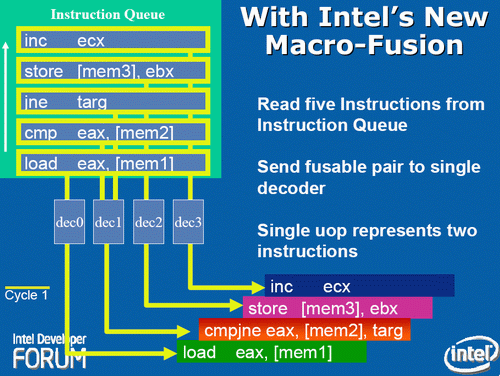
The result is that on average in a typical x86 program, for every 10 instruction, two x86 instructions (called macro-ops by Intel) are fused together. When two x86 instructions are fused together, the 4 decoders can decode 5 instructions in one cycle. The fused instruction travels down the pipeline as a single entity, and this has other advantages: more decode bandwidth, less space taken in the Out of Order (OoO) buffers, and less scheduling overhead. If Intel's "1 out of 10" claims are accurate, macro-ops fusion alone should account for an 11% performance boost relative to architectures that lack the technology.
The second clever technique already exists in the current P-M CPUs. There are a few x86 instructions which are pretty complex to perform, but which are at the same time a very typical and common x86 instruction. We are talking for example about mathematical operations where an address is referenced instead of a register. One common example is ADD [mem], EAX . This means add the content of register EAX to the content of a certain memory location (i.e. store the result back at the memory address). Store instructions which get broken down into store address and store data are another example.
In earlier designs such as the P6 (Pentium Pro, PII, PIII) architecture, these instruction would have been broken up into two or even three micro-ops. Remember that the whole philosophy behind all modern x86 CPUs, since the P6, is to decode x86 instructions into RISC-y micro-ops which are then fed to a fast RISC backend; the backend then schedules, issues, executes and retires the instructions in a smooth RISC way.
There is no way you could feed such an instruction (ADD [mem], EAX) to RISC execution units. It violates every RISC rule. RISC designs all load their data into the registers and then perform the necessary calculation on the registers.
So ADD [mem], EAX is broken down into:
Load the contents of [mem] into a register (Since Banias, the ALU and the Load operation are kept together in one micro-op. This is called micro-op fusion. This is no small feat: in older designs keeping the load and ALU operation together would result in pipeline stages that take much longer and thus lower the maximum clock frequency. (In CPU designs, the maximum clock speed is essentially determined by the slowest possible pipeline stage execution time.) Only by using bigger, smarter circuitry that can do a lot in parallel is micro-op fusion possible without lowering the clock speed significantly.MOV EBX, [mem])
An ALU operation, ADD the two registers together (ADD EBX, EAX)
Store the result back to memory (MOV [mem], EBX)
The pre-decode stage recognizes the macro-ops (or x86) instructions that should be kept together. In the decoding phase, ADD [mem], EAX results in one micro-op. Again, this means that the CPU can stuff more instructions in the same OoO buffers, increasing efficiency and improving performance.
Core versus Hammer: Decoding
All very nice, but let us take a look at what really matters: How do the 3 simple + 1 complex decoders of Core compare to the 3 complex decoders of AMD's K8 architecture?The original Athlon ("K7") has two way of decoding, Vector and Direct Path. The Vector Path decoding results in more than two RISC-like instructions (called "macro-ops" by AMD), the Direct Path in one, sometimes two macro-ops. Each of the decoders in K7 can handle both Vector Path and Direct Path decoding, but from a performance standpoint Direct Path is preferred since it results in fewer macro-ops. If you're wondering why were discussing K7 all of a sudden, just as Core is largely based off the P6 architecture, K8 is largely based off the K7 architecture.
The 3 complex decoders are powerful and can decode most x86 instructions, with few instructions requiring the Vector Path. The only downside of the K7 decoders is that some FP instructions and SSE instructions have to pass through the Vector Path. K8 has even stronger complex decoders and almost all FP and SSE instructions are also now decoded through the Direct Path decoders. This is possible as fetching and decoding takes more stages than it did in the K7; the K8 architecture is clearly more powerful when it comes to SIMD.
Obviously, Intel's Macro-op ( x86 instruction ) fusion does not exist in AMD's K8. However, micro-op fusion is available in another form. If we compare Intel's and AMD's macro-ops and micro-ops, it is easy to get confused. Take a look at the table below which explains the differences.
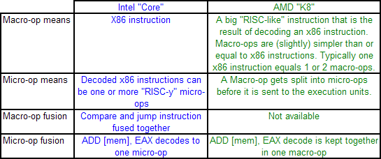
Micro-op fusion does exist in the Athlon. An ADD [mem], EAX is kept together in one macro-op as it travels through the pipeline. Therefore it will take only one place in the OoO buffers. However, the load and execute SSE/SSE2 operations can be fused on Core, while this is not the case on K8: packed SSE operations result in two macro-ops.
So how do Intel's Core and AMD's Hammer compare when it comes to decoding? It is hard to say at the moment without access to Intel's optimization manuals. However, we can get a pretty good idea. In almost every situation, the Core architecture has the advantage. It can decode 4 x86 instructions per cycle, and sometimes 5 thanks to x86 fusion. AMD's Hammer can do only 3.
The situation where AMD's 3 complex decoders can outperform Core's 1 complex + 3 simple decoders is much less likely to happen. It would happen when 3 instructions would be fetched that would have to be handled by the complex decoder of the Core CPU, but which are not too complex that the Microcode Sequencer must kick in. Since the most used x86 instructions all map to one Intel micro-op, this is pretty unlikely.


87 Comments
View All Comments
Betwon - Tuesday, May 2, 2006 - link
The data can not be used for Core -- Because it did not use the smart prefetcher.The Advanced smart prefetchers of Core's L1D have decreased the miss-rates very much. In fact, The data cache of Core --much more efficiency than K8's.
Compared with Core's smart cahce, K8's 64KB L1D is like an idiot .
Spoonbender - Tuesday, May 2, 2006 - link
How do you know? As the article said, the prefetching *might* in some cases decrease performance, even if it'll usually be an advantage. But I don't really think you have enough information to make a valid comparison. My point was simply that generally speaking, a 64KB, 2-way associative cache will have better hit rates than a 32KB 8-way associative. Of course, having fancy prefetching is always a good thing, but its effect *is* limited. If it was a huge improvement, people would have done that 8 years ago, instead of just messing with cache size and associativity.Betwon - Tuesday, May 2, 2006 - link
Your information is too old and should be updated now.Prefetcher give much improvement in reducing the miss-rate.
About 30-90% miss rate reduced.
The good prefetcher tech is one of the most important performance factors.
http://www.hpcaconf.org/hpca11/slides/hpca_inst_sl...">http://www.hpcaconf.org/hpca11/slides/hpca_inst_sl...
Betwon - Tuesday, May 2, 2006 - link
Who is James E. Smith? I think that you should know him.Data Cache Prefetching Using a Global History Buffer -- the prefetcher bring the great performance improvement! From 20-110%
abstract
http://ieeexplore.ieee.org/search/freesrchabstract...">http://ieeexplore.ieee.org/search/frees...+buffer%...
Of course, you can download the full-text pdf file, if you have a IEEE member account. I can download and view it, but can not release it.
slides ppt
http://www.ece.gatech.edu/~leehs/ECE7102/slides/ka...">http://www.ece.gatech.edu/~leehs/ECE7102/slides/ka...
Sunrise089 - Monday, May 1, 2006 - link
flak flak flakSeriously - props to the author on a good article, but if I had one comment it would be that there are length issues to trying to provide the ammount of background needed for this sort of article. I think it's best to either just draw the comparisons between the two chips, or do a full-length many thousands of words write-up on the technical importance of the various topics. I read the article, and while writen well and informative in it's conclusions, I cannot say all the background was enough to make me really understand the concepts better. For example I already knew what out-of-order execution was, but only being able to read a few hundred words more on it didn't allow me to really learn enough to understand all of the reasons why the K8 had a disadvantage in that area, and if all you wanted was for me to understand that it did indeed have the disadvanatge, you could have just said so.
JohanAnandtech - Monday, May 1, 2006 - link
It is indeed an issue I struggled with. Writing full length articles on these subjects doesn't sound like a good idea for me: I personally do not like lengthy articles either. So I tried to keep a balance between being technical and keeping it understandable.Anyway, Just ask about the points where you were lost. Especially on the OoO matters: it is much more interesting than "AMD has a disadvantage". Basically, reordering happens between the decoding and the execute phase.
Pushing loads forward helps in two ways:
1.Whenever a load fails to get it's data from the L1-cache, the CPU has to find other instructions to execute. As loads are very common, it is easier to fill the gaps than when you can not move loads before other loads.
2. If a load gets pushed forward and a L1-cache miss for that load occurs, it isn't that bad. This is very simplified, but assume the load has been pushed 5 cycles forward, and your L2-cache latency is 10, you only have to wait 5 cycles instead of 10.
Furen - Monday, May 1, 2006 - link
I'll be the grammar nazi today, lol.Last page, paragraph 5: "[...] increasing the <b>wideness</b> of each unit [...]"
Width, perhaps? "Wideness" refers to either quality or state (neither of which is discrete) while "width" also also applies to measurable fact (128-bits wide, for example). You can talk about the wideness of the units, for example, but you cannot talk about increasing their wideness...
Great article, by the way, it's been long since I've read such an enjoyable article.
emboss - Monday, May 1, 2006 - link
Just a quick note ... on page 4 you have the table with the execution unit details. There's a couple things incorrect (IMO) in the numbers.First, you list the number of double precision FLOPs per cycle. Double precision can be done with SSE, so in the K8 you can do 2 DP ADDs and 2 DP MULs every two cycles (due to the 64-bit wide datapaths), a total of 2 DP FLOPs per cycle.
Core can do two SSE operations per cycle (the two symmetric units), giving it a total of 4 DP FLOPs per cycle. The third SSE unit does not handle FP ops, but instead handles shuffles and the like.
Obviously, double both of these numbers if you want a "peak" single precision FLOPs per cycle.
If instead you were meaning about extended precision (64 bit precision, 80 bit floats) x87 operations, it's exactly the same concept as above since Core has apparently has combined SSE/x87 units (and a fully pipelined FMUL, unlike the P4). This gives both the K8 and Core 2 EP FLOPs per cycle.
Finally, you have the number of SSE units for the K7 wrong. The K7, like the K8, has two SSE units (FADD and FMUL), and the same 64 bit datapath as the K8. Of course, the K7 cannot handle SSE2, so must use x87 instructions for double precision (ie: two DP FLOPs per cycle).
Apart from that, very nice article! I've been trying to optimise SSE code for the Core processor and have had to do things by trial and error thanks to the complete void of any decent documentation from Intel. One thing in particular was that I was finding "odd" performance properties with SSE that pointed towards it having two FMUL units. Being symmetric units explains a lot!
JarredWalton - Monday, May 1, 2006 - link
See above note regarding Core Duo versus Core "Conroe". (Nice naming scheme, Intel. *grumble*) I will let Johan take care of the rest of your comment as appropriate. (His knowledge of the low level details of all of the microarchitectures discussed here definitely surpasses mine!)Unfortunately, it's not particularly surprising to find out that optimal code for Core Duo may need to be slightly tweaked in order to extract the most performance from Conroe. Still, they ought to be similar enough that you own by optimizing for Core Duo. The flipside is the optimal code for Conroe could very likely run worse on Core Duo and other processors. Such is the price of progress, I guess.
prx99 - Monday, May 1, 2006 - link
Core is not the first x86 having 4 decoders. That was AMDs K5.I remember a statement from AMD that in some design they considered adding one more decoder. It turned out to actually slow down the design because the amount of clock speed lost was not compensated for by the smaller amount of performance gained.
In my interpretation the fusion is done past the initial decoding, so there is not way more that 4 x86 ops can be decoded in a clock cycle (I'm referring to the "4+1" figure). The profit from fusion is not in the decoding stage but in the out of order engine.
At AMDs, the "1 branch per cycle" rule is limited to branches seen by the predictor. A branch which is generally not taken is invisible to the prediction engine and therefore free.
The original P4 indeed had a L1 latency of 2. The major P4 redesign in Prescott however increased it to 3.
Load/store reordering is already done by the P4, but the penalty from a misprediction is fairly high. This is the drawback of any kind of prediction, whether branches or memory access: It speeds up things when being correct, but slows them down quite a bit more when not. This was the general picture seen in the P4: many applications were sped up by some amount, but some suffered greatly because they systematically fooled the P4's engines.
Gruss, Andreas