Smarter Decoding
Similar to the K8 architecture, Core pre-decodes instructions that are fetched. Pre-decode information includes instruction length and decode boundaries.A first for the x86 world, the Core architecture is equipped with four x86 decoders, 3 simple decoders and 1 complex decoder. The task of the decoders - for all current x86 CPUs - is not only to decipher the incoming instruction (opcode, addresses), but also to translate the 1 to 15 byte variable length x86 instructions into - easier to schedule and execute - fixed length RISC-like instructions (called micro-ops).
The most common x86 instructions are translated into a single micro-op by the 3 simple decoders. The complex decoder is responsible for the instructions that produce up to 4 micro-ops. The really long and complex x86 instructions are handled by a microcode sequencer. This way of handling the complex most CISC-y instructions has been adopted by all modern x86 CPU designs, including the P6, Athlon (XP and 64), and Pentium 4.
There is still more to the Core decoders. The first clever technique is macro-op fusion. It makes it possible for two relatively common x86 instructions to be fused into a single instruction. For example, the x86 compare instruction (CMP) is fused with a jump (JNE TARG). These instructions are typically the assembler result of a compiled if-then-else statement.
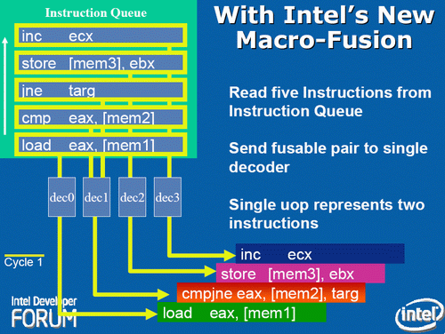
The result is that on average in a typical x86 program, for every 10 instruction, two x86 instructions (called macro-ops by Intel) are fused together. When two x86 instructions are fused together, the 4 decoders can decode 5 instructions in one cycle. The fused instruction travels down the pipeline as a single entity, and this has other advantages: more decode bandwidth, less space taken in the Out of Order (OoO) buffers, and less scheduling overhead. If Intel's "1 out of 10" claims are accurate, macro-ops fusion alone should account for an 11% performance boost relative to architectures that lack the technology.
The second clever technique already exists in the current P-M CPUs. There are a few x86 instructions which are pretty complex to perform, but which are at the same time a very typical and common x86 instruction. We are talking for example about mathematical operations where an address is referenced instead of a register. One common example is ADD [mem], EAX . This means add the content of register EAX to the content of a certain memory location (i.e. store the result back at the memory address). Store instructions which get broken down into store address and store data are another example.
In earlier designs such as the P6 (Pentium Pro, PII, PIII) architecture, these instruction would have been broken up into two or even three micro-ops. Remember that the whole philosophy behind all modern x86 CPUs, since the P6, is to decode x86 instructions into RISC-y micro-ops which are then fed to a fast RISC backend; the backend then schedules, issues, executes and retires the instructions in a smooth RISC way.
There is no way you could feed such an instruction (ADD [mem], EAX) to RISC execution units. It violates every RISC rule. RISC designs all load their data into the registers and then perform the necessary calculation on the registers.
So ADD [mem], EAX is broken down into:
Load the contents of [mem] into a register (Since Banias, the ALU and the Load operation are kept together in one micro-op. This is called micro-op fusion. This is no small feat: in older designs keeping the load and ALU operation together would result in pipeline stages that take much longer and thus lower the maximum clock frequency. (In CPU designs, the maximum clock speed is essentially determined by the slowest possible pipeline stage execution time.) Only by using bigger, smarter circuitry that can do a lot in parallel is micro-op fusion possible without lowering the clock speed significantly.MOV EBX, [mem])
An ALU operation, ADD the two registers together (ADD EBX, EAX)
Store the result back to memory (MOV [mem], EBX)
The pre-decode stage recognizes the macro-ops (or x86) instructions that should be kept together. In the decoding phase, ADD [mem], EAX results in one micro-op. Again, this means that the CPU can stuff more instructions in the same OoO buffers, increasing efficiency and improving performance.
Core versus Hammer: Decoding
All very nice, but let us take a look at what really matters: How do the 3 simple + 1 complex decoders of Core compare to the 3 complex decoders of AMD's K8 architecture?The original Athlon ("K7") has two way of decoding, Vector and Direct Path. The Vector Path decoding results in more than two RISC-like instructions (called "macro-ops" by AMD), the Direct Path in one, sometimes two macro-ops. Each of the decoders in K7 can handle both Vector Path and Direct Path decoding, but from a performance standpoint Direct Path is preferred since it results in fewer macro-ops. If you're wondering why were discussing K7 all of a sudden, just as Core is largely based off the P6 architecture, K8 is largely based off the K7 architecture.
The 3 complex decoders are powerful and can decode most x86 instructions, with few instructions requiring the Vector Path. The only downside of the K7 decoders is that some FP instructions and SSE instructions have to pass through the Vector Path. K8 has even stronger complex decoders and almost all FP and SSE instructions are also now decoded through the Direct Path decoders. This is possible as fetching and decoding takes more stages than it did in the K7; the K8 architecture is clearly more powerful when it comes to SIMD.
Obviously, Intel's Macro-op ( x86 instruction ) fusion does not exist in AMD's K8. However, micro-op fusion is available in another form. If we compare Intel's and AMD's macro-ops and micro-ops, it is easy to get confused. Take a look at the table below which explains the differences.
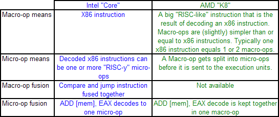
Micro-op fusion does exist in the Athlon. An ADD [mem], EAX is kept together in one macro-op as it travels through the pipeline. Therefore it will take only one place in the OoO buffers. However, the load and execute SSE/SSE2 operations can be fused on Core, while this is not the case on K8: packed SSE operations result in two macro-ops.
So how do Intel's Core and AMD's Hammer compare when it comes to decoding? It is hard to say at the moment without access to Intel's optimization manuals. However, we can get a pretty good idea. In almost every situation, the Core architecture has the advantage. It can decode 4 x86 instructions per cycle, and sometimes 5 thanks to x86 fusion. AMD's Hammer can do only 3.
The situation where AMD's 3 complex decoders can outperform Core's 1 complex + 3 simple decoders is much less likely to happen. It would happen when 3 instructions would be fetched that would have to be handled by the complex decoder of the Core CPU, but which are not too complex that the Microcode Sequencer must kick in. Since the most used x86 instructions all map to one Intel micro-op, this is pretty unlikely.


87 Comments
View All Comments
spinportal - Monday, May 1, 2006 - link
Definitely a great treasure of an article to find on a monday morning detailing the Core architecture that the world is drooling for in June. I wonder what kind of simulation micro-arch software Intel and AMD use, as I remember the days doing my Masters, playing with Intel's Hypercube simulator (grav sim, fish & shark AI sim) and writing my own macro level visual-cpu execution simulator.JarredWalton - Monday, May 1, 2006 - link
I won't say it's a quick fix, but just as Core is a derivative of P6, AMD could potentially just get some better OoO capabilities into K8 and get some serious performance improvements. Their current inability to move loads forward much (if at all) makes them even more dependent on RAM latency. You could even say that they *needed* the IMC to improve performance, but still L2 latency is far better than RAM latency, and cutting down L2 latency hit from 12 cycles to say 6 cycles (if you can do the load 6 cycles early) would have to improve performance. Loads happen "all the time" in ASM, so optimizing their performance can pay huge dividends.I'm going to catch flak for this, but basically Intel has more elegant designs than AMD in several areas. It comes from throwing billions of dollars at the problems. Better L1 cache? Yup - 8-way vs. 2-way is pretty substantial; 256-bit vs. 128-bit is also substantial. Better specialization of hardware? Yeah, I have to give them that as well: rather than just using three ALUs, they often take the path of having a few faster ALUs to handle the common cases.
Really, the only reason AMD was able to catch (and exceed) Intel performance was because Intel got hung up on clock speeds. They basically let marketing dictate chip design to engineering - which is never good, IMO, at least not in the long run. Even NetBurst still has some very interesting design features (double-pumped ALUs, specialization of functional units, trace cache), and if nothing else it served as a good lesson on how far you can push clock speeds and pipeline lengths before you start encountering some serious problems. I would have loved to see Northwood tweaked for 90nm and 65nm, personally - 31+8 pipeline stages was just hubris, but 20+8 with some other tweaks could have been interesting.
Here's hoping AMD can make some real improvements to their chips sooner rather than later. Intel Core is looking very strong right now, and I would rather have close competition than a 20% margin of victory like we've been seeing lately. (First with AMD K8 beating NetBurst, and now it looks like Conroe is going to turn the tables.)
Regs - Wednesday, June 7, 2006 - link
Okcourse you will catch flack. It's an opinion.My opinion is Intel is more innovative or even compromising
while AMD is more intuitive.
Spoonbender - Monday, May 1, 2006 - link
"8-way 32kb * 2 L1 should in theory exceed the hitrate of K8's 2-way 64kb * 2 L1."It should? I'd like to see some sources on that. From what I've seen, the 64KB cache still has an advantage there, with a hitrate not much below that of a 64KB/8-way.
Also, I disagree that Intel's CPU's are generally more elegant. First, their L1 cache isn't neccesarily "better" (see above). Of course, the 256 vs 128 bit bandwidth is a big factor, however.
Specialization in hardware? Is that elegant? I'd say there's a certain elegance in making a general solution as well, as opposed to specializing everything to the point where you're screwed if the code you have to execute isn't 100% optimal.
And I definitely think AMD's distributed reservation stations are more elegant than the central one used by Intel. Same goes with the usual HyperTransport vs FSB story.
There are a few other really elegant features of the K8 that I haven't seen duplicated in Core.
So overall, I don't see the big deal with "elegance". Both architectures have plenty of elegant features. However, the K8 is definitely aging, and will have problems keeping up with Conroe.
But then again, the K8 die is tiny in comparison. They've got plenty of space for improvements.
Really looking forward to
1) Being able to get a Merom-powered laptop, and
2) Seeing what AMD comes up with next year.
IntelUser2000 - Monday, May 1, 2006 - link
Tiny?? 199mm2 for 2x1MB cache K8 at 90nm is tiny?? Ok there. Conroe with 4MB cache is around 140mm2 die size.
http://www.aceshardware.com/forums/read_post.jsp?i...">http://www.aceshardware.com/forums/read_post.jsp?i...
Even compairing against Intel's SRAM size for 90nm and 65nm comparison, at 90nm, Conroe would be 250mm2. In Prescott, 1MB L2 cache takes 16-17mm2. 250mm2-32mm2=218mm2.
And Intel didn't to shrinks that are relative to SRAM sizes. In comparison for Cedarmill and Prescott 2M, which are same cores essentially.
Prescott 2M: 135mm2
Cedarmill: 81mm2
Only difference being process size, the comparison is 0.6.
Conroe at 90nm would have been 233mm2, which is compact as X2 per core.
Spoonbender - Tuesday, May 2, 2006 - link
Okay, I guess I should have said that at the same process size, it is tiny. I meant that when AMD gets around to migrating to 65nk as well, they'll have a smaller core (assuming no big changes to the chip), which gives them plenty (some?) of room for improvement.[quote]
Conroe at 90nm would have been 233mm2, which is compact as X2 per core.
[/quote]
But in absolute terms, still bigger than an Athlon X2. Which means AMD has some space for improvement. That was my only point. I guess I should have been more clear. ;)
coldpower27 - Wednesday, May 3, 2006 - link
Yes, if using the 0.6 Factor for Brisbane the 65nm Athlon 64x2 it will be around 132mm2 assuming no changes over the 220mm2 Windsor DDR2 Athlon64x2. 199mm2 is only for Toledo which is reaching end of life and can no longer be used as a comparison. And it's irrelevent to compare to Conroe on what it would be on 90nm as it never was built on 90nm technology to begin with.Conroe is looking to be ~14x mm2 with the x=0-9. Yes if you can compare them at the same process nodes considering the Conroe will only be competing with the 65nm Dual Core Athlon 64x2 in the second half of it's lifetime.
JumpingJack - Tuesday, May 2, 2006 - link
Nice analysis, the current AMD X2 dual cores are about 1.5 to 2.0 X the size of Intel dual cores (on 65 nm), this is where 65 nm adds such a benefit. Conroe will come in around 140 mm^2 as you said. Yohna at 2 meg shared is 90 mm^2, less than 1/2 the X2.Right now, cost wise in Si realestate AMD is more expensive.
BitByBit - Monday, May 1, 2006 - link
Here is a good article on processor cache:
http://en.wikipedia.org/wiki/CPU_cache">http://en.wikipedia.org/wiki/CPU_cache
If you scroll down to the miss-rate vs. cache size graph, you can see that an 8-way 64Kb cache has a miss-rate less than one-tenth the miss-rate of a 2-way 64Kb cache.
An 8-way 64Kb * 2 L1 would probably be too difficult to implement, given the time it would take to search. However, according to the relationships shown by that graph, increasing the Athlon's L1 associativity to 4-ways could yield a nice boost in hitrate and consequently performance.
Spoonbender - Monday, May 1, 2006 - link
And of course, we all know wikipedia is the ultimate source of all truth and knowledge... ;)Keep in mind that this graph only shows the Spec2000 benchmark (and only the integer section, at that). That's far from being representative of all code.
According to http://www.amazon.com/gp/product/1558605967/002-28...">http://www.amazon.com/gp/product/155860...-2818646... which, in my experience is pretty damn good, the missrates are as follows *in general*:
32KB, 8-way: 0.037
64KB, 2-way: 0.031
64KB 8-way: 0.029
But yeah, of course improving the Athlon's cache would help. But it's not the first place I'd look to optimize. For one thing, making it more complex would, as seen above, not yield a significantly lower hitrate, but it would slow the cache down, either forcing them to increase its latency, or limiting the frequency potential of the cpu as a whole. The cache bandwidth might be a better candidate for improvement. Or some of the actual cpu logic. Or the L2 cache size. I think the L1 cache is pretty healthy on the K8 already.