An AMD Update: Fab 36 Begins Shipments, Planning for 65nm and AM2 Performance
by Anand Lal Shimpi on April 4, 2006 11:00 AM EST- Posted in
- CPUs
AMD also gave us a brief update on 45nm, stating that they have successfully produced a SRAM test wafer at 45nm. It's very popular to produce a wafer full of SRAM chips as you're bringing up and validating any new process, since the circuits are simple enough to actually make the chips producable but complex enough to get useful feedback on your process from the test wafer.
AMD's 45nm SRAM test wafer follows a little over 3 months after Intel demonstrated a similar 45nm test wafer. The benchmark when producing a wafer of SRAM is how small you're able to produce each SRAM cell. At 45nm Intel was able to achieve a 0.346 square micron SRAM cell size compared to AMD's 0.370 square micron SRAM cells. Intel's advantage in SRAM cell size is nothing new, as they have been doing so in previous process technologies as well. The advantage in SRAM cell size is one reason why you often see Intel more eager to equip its CPUs with larger L2 caches; obviously with no on-die memory controller, Intel also often benefits much more from a larger L2 cache than AMD in the first place.
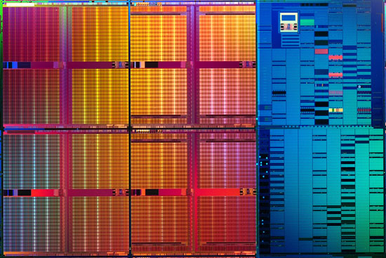
Intel's 45nm SRAM test vehicle - 0.346 sq micron cell size
Today's update had nothing to do with Socket-AM2 or AMD's transition to DDR2, but we do have some news with regards to that as well. As you've undoubtedly heard and maybe even seen elsewhere, AMD's AM2 platform has not been performing very well in development over these past couple of months. Just before IDF, AM2 samples were still performing lower than their Socket-939 counterparts, which was beginning to worry us and AMD's parters a bit. However we're excited to report that AM2 performance has finally started exceeding that of Socket-939. The performance gains we've been hearing and seeing are generally 5% or lower at the same clock speeds using DDR2-800, but it's still very early. The main point to take home is while the final verdict is still not out, AM2 is at least starting to look like more of an upgrade and not what we saw with Intel's DDR to DDR2 transition almost 2 years ago.
There's still a lot that AMD does have to give us however, including a more specific roadmap of what comes after their DDR2 transition. AMD's Phil Hester has publicly stated that once AM2 launches it will be more forthcoming with information on future architecture revisions, we can only hope so because over the past 12 months Intel has put the pressure on AMD to really start talking about the future.
The good news today is that AMD is truly growing as a company. By 2008 AMD hopes to be able to double its yearly shipments of microprocessors, and it's finally got manufacturing capacity to do just that. For the past few years AMD has held technological and performance advantages over Intel, now it's time for AMD to play catchup on the manufacturing side. AMD has a long way to go before being anywhere close to Intel's manufacturing abilities, but it is in a very good place today.


68 Comments
View All Comments
Viditor - Friday, April 7, 2006 - link
Of course it can...don't you read reviews?
If you read http://www.xbitlabs.com/articles/cpu/display/sempr...">this X-Bit review (granted there aren't a lot of reviews on Sempron), you'll see it runs neck and neck (and in many cases better) with the A64 3000+ which Anand directly compared to the 805 http://www.anandtech.com/cpuchipsets/showdoc.aspx?...">here.
As Anand said in his conclusion:
"Gamers looking for a temporary upgrade should honestly look to the Athlon 64 3000+ instead, as very few games have boarded the dual train as of now"..."if you are a multitasker or run multithreaded applications, and you want a great low cost solution, then the Pentium D 805 makes a wonderful stepping stone to a future AM2 or Conroe platform. If you're a gamer that doesn't care about multitasking while gaming, the Athlon 64 3000+ is still a strong value"
In addition, if you look at the power usage page of Anand's review, you'll note that the 805 requires a power plant of it's own...:) (j/k)
blackbrrd - Tuesday, April 4, 2006 - link
Bullshit ;)Anandtech was one of the first review sites to match the Opteron up vs the Xeon, which showed Opteron spanking Xeons. Haven't seen anything like those reviews from any other sites.
hans007 - Tuesday, April 4, 2006 - link
they have used a lot of vague terminology.i.e. our wafer yields at 300mm are equal to 200mm.
that means, what?
that they get the same number of cpus out of 300mm and 200mm. or the percenteage of the wafer yield?
they also have no 65nm demos at all even though they claim to be sampling the cpus. and they claim 40% better transistor performance, but that probably just means it say uses up less power not switching faster.
so it all depends on just the exact details of what that all means.
AnnonymousCoward - Saturday, April 8, 2006 - link
"Yield" refers to the percentage of good die.40% better transistor performance isn't merely talking about power. Performance means performance. It's also not saying the CPU is going to be 40% faster. There's propagation delays involved with transistor circuits, and some low level figure will be sped up by 40% (I don't know if it's rise/fall times, propagation delay, switching frequency, etc).
Calin - Wednesday, April 5, 2006 - link
As a 300mm wafer has more than twice the size of a 200mm wafer, they should produce twice as much processors from a 300mm wafer. Maybe more, as less space is lost on the sides.Anyway, why they don't make the wafers square? that would decrease the area lost on sides
stephenbrooks - Thursday, April 6, 2006 - link
I think they should make the chips round.Zoomer - Sunday, April 9, 2006 - link
That will be even worse, unless 1 chip == 1 wafer. And that's insane.eetnoyer - Wednesday, April 5, 2006 - link
I guess you don't know how wafers are made. The silicon is originally made sort of like homemade rock candy (Put a string tied to a pencil into a jar of hot, sugar-saturated water) and thus comes out in a columnar shape (I know, very rough analogy). After that, the wafers are made by taking slices off of the column. I suppose they could square the columns before slicing, but then there would be alot of waste, the cost of which would still be passed onto the chip maker. Much more efficient to just get that extra production out of the circular wafer.....it doesn't really cost any extra.Calin - Thursday, April 6, 2006 - link
No, I didn't knew. Thanks for the explanation.I remember I heard about diamond "wafers" that were made by growing a rectangular substrate - and once it was thick enough, they would cut it in several smaller slices. The result would be a "brick". I somehow assumed silicon would be the same
menting - Tuesday, April 4, 2006 - link
exactly what I was thinking.also, that's comparing the 300mm and 200mm wafers at 90nm process only, which isn't too much of a feat to accomplish.
when the 300mm goes to 65nm process, the yield (% die/waf) will definitely go down some, how much we probably will never know. it could go down enough that a 300mm wafer will initially produce only about the same or a little more number of dies per wafer than the 200mm at 90nm does.
Basically this announcement regarding yields isn't saying much except for the expected.