Understanding the Cell Microprocessor
by Anand Lal Shimpi on March 17, 2005 12:05 AM EST- Posted in
- CPUs
Blueprint for a High Performance per Transistor CPU
Given that Cell was designed with a high performance per transistor metric in mind, its architecture does serve as somewhat of a blueprint for the technologies that result in the biggest performance gains, at the lowest transistor counts. Now that we’ve gone through a lot of the Cell architecture, let’s take a look back at what some of those architectural decisions are:1. On-die memory controller
We’ve seen this with the Athlon 64, but an on-die memory controller appears to be one of the best ways to improve overall performance, at minimal transistor expenditure. Furthermore, we also see the use of Rambus’ XDR memory instead of conventional DDR, as the memory of choice for Cell. High frequencies and high bandwidth are what Cell thrives on, and for that, there’s no substitute but Rambus’ technology.
2. SMT
On-die multithreading has also been proven to be a good way of extracting performance at minimal transistor impact. Introducing Hyper Threading to the Pentium 4’s core required a die increase of less than 5%, just to give you an idea of the scale of things. The performance benefits to SMT will obviously vary depending on the architecture of the CPU. In the case of the Pentium 4, performance gains ranged from 0 - 20%. In the case of the in-order PPE core of Cell, the performance gains could be even more. Needless to say, if implemented well, and if proper OS/software support is there, SMT is a feature that makes sense and doesn’t strain the transistor budget.
3. Simpler, in-order, narrow-issue core - but lots of them
This next design decision is more controversial than the first two, simply because it goes against the design strategies of most current generation desktop microprocessors that we’re familiar with. By making the PPE and SPEs 2-issue only, each individual core still remains a manageable size. Narrower cores obviously sacrifice the ability to extract ILP, but doing so allows you to cram more cores onto a single die - highlighting the ILP for TLP sacrifice that the Cell architects have made.
Getting rid of the additional logic and windows needed for an out-of-order core helps further reduce transistor count, but at the expense of making sure that you have a solid compiler and/or developers that are willing to deal with more of the architecture’s intricacies to achieve good performance.
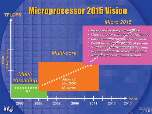
Looking at Intel’s roadmap for Platform 2015, the type of microprocessors that they’re talking about are eerily Cell-like - a handful of strong general purpose cores surrounded by smaller cores, some of which are more specialized hardware.


70 Comments
View All Comments
Houdani - Friday, March 18, 2005 - link
I think I missed something fundamental.Can the SPEs be addressed directly by software, or do they have to be fed all of their instructions by the PPE?
If they DO have to be fed be the PPE, I fail to see how the PPE can possibly feed them enough to keep them all working concurrently.
Someone throw me a bone here.
suryad - Friday, March 18, 2005 - link
I thought the G5 was a POWER5 proc. But I could of course be wrong. All I can say is the Cell definitely intriguing as it may be will have a rough road ahead of it and I am quite surprised that these large corporations invested so much in it, cutting edge though it might be. And as for the current forseeable future, I think when multi-core FX processors from AMD comes out, I do not believe there will be anything more devastating than that. Especially once they hit the 3 Ghz barrier with multi-cores enabled and faster DDR2-3 or even RAMBUS memory capabilities.tipoo - Thursday, December 3, 2015 - link
No, G5 was 970 based.Questar - Friday, March 18, 2005 - link
#50,Yes the G5 is a POWER4 derivitive.
Since you were wrong on that, don't think that you know what is significant about the design of POWER5. There were major architechture changes made to the processor.
fitten - Friday, March 18, 2005 - link
The only things new about Cell is its target market and being a single chip. The article mentions the TI DSP chip, but there were other similar architectures as well. One example that I'm familiar with is the MAP1310 board by CSPI. Back then, processes weren't good enough to put all the cores on a single chip but the basic architecture is the same - a PPC core to do the 'normal' stuff and two quad-core DSPs (SHARC) to do the 'work'. This board wasn't successful because it was considered too hard to program to get the performance it promised.... and this opinion is from people who live/breathe real-time systems and multiprocessing codes.The only thing new about Cell is that a) it's all on one chip now and b) the target market is a general marketplace and not a niche.
scrotemaninov - Friday, March 18, 2005 - link
#48. OK, I was under the impression that the G5 was based on the POWER5. You're saying it's based on the POWER4 instead?And the POWER4 and POWER5 aren't really "completely different chips" in the same way that the P4 and P3 are different chips, or in the way that the P4 and the Opteron are different chips. I can give you a list of the differences if you want. Start at http://www.elet.polimi.it/upload/sami/architetture...
The POWER5 is designed to not only be completely compatible with the POWER4 but to also to support all the optimisations from the POWER4. The only things of significance they've done is a) move the L3 cache controller on chip; b) change the various branch predictors to bimodal instead of 1-bit; c) increase the associativity and size of the caches.
Anyway, this is going off topic now...
Jacmert - Friday, March 18, 2005 - link
Rofl. Computer engineering and VLSI design. Gotta love those NMOS/PMOS transistor circuits.I never thought that I'd see stuff from my textbook explained on anandtech.com
saratoga - Friday, March 18, 2005 - link
"#38. You're right that the G5 is a derivative of the POWER5. The POWER5 is dual core, each core with 2way SMT giving a total of 4 'visible' cpus to the OS. The G5 is simply a single core version of the same thing."Err no its not. POWER4 != POWER5. Hence the different names ;)
They're completely different chips.
"Well scrotemaninov I am not disputing that the POWER architecture by IBM is brilliantly done. IBM is definitely one of those companies churning out brilliant and elegant technology always in the background.
But my problem with the POWER technology is from what I understand very limitedly, is that the POWER processors in the Mac machines are a derivative of that architecture right? Why the heck are they so damn slow then?
I mean you can buy an AMD FX 55 based on the crappy legacy x86 arch and it smokes the dual 2.5 GHz Macs easily!! Is it cause of the OS? Because so far from what I have seen, if the Macs are any indication of the performance capabilities of the POWER architecture, the Cell will not be a big hit.
I did read though at www.aceshardware.com benchmark reviews of the POWER5 architecture with some insane number of cores if I recall correctly and the benchmarks were of the charts. They are definitely not what the Macs have installed in them..."
There are slow memeory systems and then theres the one used on the G5. I've heard that you can put 8 Opterons together and still get average access times across all 8 cores that are better then a single G5. Thats probably a good part of the reason the G5 was so much slower then many people thought it would be. The rest is mainly IBM's trouble making them, and their inability to ramp clock speed like they planned on.
scrotemaninov - Friday, March 18, 2005 - link
#38. You're right that the G5 is a derivative of the POWER5. The POWER5 is dual core, each core with 2way SMT giving a total of 4 'visible' cpus to the OS. The G5 is simply a single core version of the same thing.As for the performance, Opteron is pretty much unbeatable for integer-bound applications. Itanium2 is unbeatable for FP applications. POWER5 is somewhere in the middle.
Most desktop applications are going to be integer bound. So it's not at all surprising that you find the G5 'slow' in that respect in comparison to the FX55. Plus, and this is the whole problem with the CELL, there's no point putting dual CPUs in there unless you can utilise them properly. If you have one process going flat out trying to run a heavy application and it's single threaded then you're only using about 1/4 of the CPUs you've bought for that application (for a dual G5 2.5), whereas the Opterons and FX55 stuff is more designed around quick, single threaded applications.
dmens - Friday, March 18, 2005 - link
psuedo-pmos wtf? That's domino logic, it's been around forever, and it's definitely not efficient in terms of power. Oh, and it takes forever to verify timing.