ATI Radeon X800 Pro and XT Platinum Edition: R420 Arrives
by Derek Wilson on May 4, 2004 10:28 AM EST- Posted in
- GPUs
Depth and Stencil with Hyper Z HD
In accordance with their "High Definition Gaming" theme, ATI is calling the R420's method of handling depth and stencil processing Hyper Z HD. Depth and stencil processing is handled at multiple points throughout the pipeline, but grouping all this hardware into one block can make sense as each step along the way will touch the z-buffer (an on die cache of z and stencil data). We have previously covered other incarnations of Hyper Z which have done basically the same job. Here we can see where the Hyper Z HD functionality interfaces with the rendering pipeline:
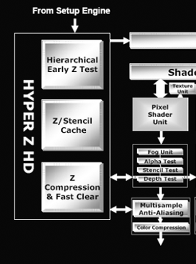
The R420 architecture implements a hierarchical and early z type of occlusion culling in the rendering pipeline.
With early z, as data emerges from the geometry processing portion of the GPU, it is possible to skip further rendering large portions of the scene that are occluded (or covered) by other geometry. In this way, pixels that won't be seen don't need to run through the pixel shader pipelines and waste precious resources.
Hierarchical z indicates that large blocks of pixels are checked and thrown out if the entire tile is occluded. In R420, these tiles are the very same ones output by the geometry and setup engine. If only part of a tile is occluded, smaller subsections are checked and thrown out if possible. This processing doesn't eliminate all the occluded pixels, so pixels coming out of the pixel pipelines also need to be tested for visibility before they are drawn to the framebuffer. The real difference between R3xx and R420 is in the number of pixels that can be gracefully handled.
As rasterization draws nearer, the ATI and NVIDIA architectures begin to differentiate themselves more. Both claim that they are able to calculate up to 32 z or stencil operations per clock, but the conditions under which this is true are different. NV40 is able to push two z/stencil operations per pixel pipeline during a z or stencil only pass or in other cases when no color data is being dealt with (the color unit in NV40 can work with z/stencil data when no color computation is needed). By contrast, R420 pushes 32 z/stencil operations per clock cycle when antialiasing is enabled (one z/stencil operation can be completed per clock at the end of each pixel pipeline, and one z/stencil operation can be completed inside the multisample AA unit).
The different approaches these architectures take mean that each will excel in different ways when dealing with z or stencil data. Under R420, z/stencil speed will be maximized when antialiasing is enabled and will only see 16 z/stencil operations per clock under non-antialiased rendering. NV40 will achieve maximum z/stencil performance when a z/stencil only pass is performed regardless of the state of antialiasing.
The average case for NV40 will be closer to 16 z/stencil operations per clock, and if users don't run antialiasing on R420 they won't see more than 16 z/stencil operations per clock. Really, if everyone begins to enable antialiasing, R420 will begin to shine in real world situations, and if developers embrace z or stencil only passes (such as in Doom III), NV40 will do very well. The bottom line on which approach is better will be defined by the direction the users and developers take in the future. Will enabling antialiasing win out over running at ultra-high resolutions? Will developers mimic John Carmack and the intensive shadowing capabilities of Doom III? Both scenarios could play out simultaneously, but, really, only time will tell.


95 Comments
View All Comments
Pumpkinierre - Wednesday, May 5, 2004 - link
Sorry, scrub that last one. I couldnt help it. I will reform.Pumpkinierre - Wednesday, May 5, 2004 - link
So, which is better: a64 at 2Gig or P4 at 3.2?jibbo - Wednesday, May 5, 2004 - link
"Zobar is right; contra Jibbo, the increased flexibility of PS3 means that for many 2.0 shader programs a PS3 version can achieve equivalent results with a lesser performance hit."I think you're both still missing my point. There is nothing that says PS3.0 is faster than PS2.0. You are both correct that it has to potential to be faster, though you both assume that a first generation PS3.0 architecture will perform at the same level as a refined PS2.0 architechture.
PS3.0 is one of the big reasons that nVidia's die size and transistor count are bigger than ATI's. The additional power drain (and consequently heat dissipation) of those 40M transistors also helps to limit the clock speeds of the 6800. When you're talking about ALU ops per second (which dominate math-intensive shaders), these clock speeds become very important. A lot of the 6800's speed for PS3.0 will have to be found in the driver optimizations that will compile these shaders for PS3.0. Left to itself, ATI's raw shader performance still slaughters nVidia's.
They both made trade-offs, and it seems that ATI is banking that PS3.0 won't be a dealbreaker in 2004. Only time will tell....
Phiro - Wednesday, May 5, 2004 - link
K, I found the $400M that the CEO claimed. He also claimed $400M for the NV3x core as well. It seemed more as a boast than anything, not particularly scientific or exact.In any case, ATI supposedly spent $165-180M last year (2003) on R&D, with an estimated increase of 100% for this year. How long has the 4xx core been in development?
Regardless, ultimately we the consumers are the winners. Whether or not the R&D spent pans out will play out over the next couple years, as supposedly the nv4x core has a 24 month lifespan.
413xram - Wednesday, May 5, 2004 - link
If you watch nvidia's launch video on their site they mention the r&d costs for their new card.RyanVM - Wednesday, May 5, 2004 - link
What ever happened to using ePSXe as a video card benchmark?Phiro - Wednesday, May 5, 2004 - link
Well, Nvidia may have spent $400M on this (I've never seen that number before but we'll go with it I guess) but they paid themselves for the most part.ATI's cost can't be too trivialized - didn't they drop a product design or two in favor of getting this out the door instead? And any alteration in the architecture of something doesn't really qualify as a hardware "refresh" in my book - a hardware refresh for an OEM consists of maybe one speed notch increase in the RAM, new bios, larger default HD, stuff like that. MLK is what Dell used to call it - Mid Life Kick.
retrospooty - Wednesday, May 5, 2004 - link
"Precisely. By the time 512mb is useful, the card will be too slow for it to matter, and you'd need a new card any way."True...
Both cards perform great, both have wins and losses depending on the game. The deciding factor will be price and power requirements.
Since prices will adjust downward, at a fairly equal rate, that leaves power. With Power requirements being so incredibly high with the NV40, that leans me toward ATI.
413xram also has a good point above. For Nvidia, this is a 400 million dollar new chip design. For ATI, this was a refresh of an old design to add 16 pipes, and a few other features. After the losses NV took with the heavily flawed NV30 and 35 , they need a financial boom, and this isnt it.
mattsaccount - Wednesday, May 5, 2004 - link
There are no games available today that use 256mb of video RAM, let alone 512mb. Even upper-high-end cards routinely come with 128mb (e.g. Geforce FX 5900, Radeon 9600XT). It would not make financial sense for a game developer to release a game that only a small fraction of the community could run acceptably.>> I have learned from the past that future possibilties of technology in hardware does nothing for me today.
Precisely. By the time 512mb is useful, the card will be too slow for it to matter, and you'd need a new card any way.
413xram - Wednesday, May 5, 2004 - link
#64 Can you explain "gimmick"?