ATI Radeon X800 Pro and XT Platinum Edition: R420 Arrives
by Derek Wilson on May 4, 2004 10:28 AM EST- Posted in
- GPUs
The Pixel Shader Engine
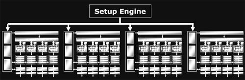
On par with what we have seen from NVIDIA, ATI's top of the line card is offering a GPU with a 16x1 pixel pipeline architecture. This means that it is able to render up to 16 single textured pixels in parallel per clock. As previously alluded to, R420 divides its pixel pipes into groups of four called quads. The new line of ATI GPUs will offer anywhere from one to four quad pipelines. The R3xx architecture offers an 8x1 pixel pipeline layout (grouped into two quad pipelines), delivering half of R420's pixel processing power per clock. For both R420 and R3xx, certain resources are shared between individual pixel pipelines in each quad. It makes a lot of sense to share local memory among quad members, as pixels near eachother on the screen should have (especially texture) data with a high locality of reference. At this level of abstraction, things are essentially the same as NV40's architecture.
Of course, it isn't enough to just look how many pixel pipelines are available: we must also discover how much work each pipeline is able to get done. As we saw in our final analysis of what went wrong with NV3x, the internals of a shader unit can have a very large impact on the ability of the GPU to schedule and execute shader code quickly and efficiently.
At our first introduction, the inside of R420's pixel pipeline was presented as a collection of 2 vector units, 2 scalar units, and one texture unit that can all work in parallel. We've seen the two math and one texture layout of NV40's pixel pipeline, but does this mean that R420 will be able to completely blow NV40 out of the water? In short, no: it's all about what kind of work these different units can do.
Lifting up the hood, we see that ATI has taken a different approach to presenting their architecture than NVIDIA. ATI's presentation of 2 vector units (which are 3 wide at 72bits), 2 scalar units (24bits), and a texture unit may be more reflective of their implementation than what NVIDIA has shown (but we really can't know this without many more low level details). NVIDIA's hardware isn't quite as straight forward as it may end up looking to software. The fact is that we could look at the shader units in NV40's pixel pipeline in the same way as ATI's hardware (with the exception of the fact that the texture unit shares some functionality with one of the math units). We could also look at NV40 architecture as being 4 2-wide vector units or 2 4-wide vector units (though this is still an over simplification as there are special cases NVIDIA's compiler can exploit that allow more work to be done in parallel). If ATI had decided to present it's architecture in the same way as NVIDIA, we would have seen 2 shader math units and one completely independent texture unit.
In order to gain better understanding, here is a diagram of the parallelism and functionality of the shader units within the pixel pipelines of R420 and NV40:
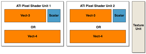
ATI has essentially three large blocks that can push up to 5 operations per clock cycle
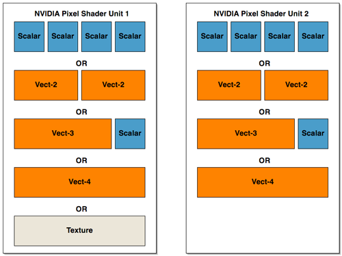
NV40 can be seen two blocks of a more amorphous configuration (but there are special cases that allow some of these parts to work at the same time within each block.
Interestingly enough, there haven't been any changes to the block diagram of a pixel pipeline at this level of detail from R3xx to R420.
The big difference in the pixel pipe architectures that gives the R420 GPU a possible upper hand in performance over NV40 is that texture operations can be done entirely in parallel with the other math units. When NV40 needs to execute a texture operation, it looses much of its math processing power (the texturing unit cannot operate totally independently of the first shader unit in the NV40 pixel pipeline). This is also a feature of R3xx that carried over to R420.
![]()
Understanding what this all means in terms of shader performance depends on the kind of code developers end up writing. We wanted to dedicate some time to hand mapping some shader code to both architecture's pixel pipelines in order to explain how each GPU handled different situations. Trial and error have led us to the conclusion that video card drivers have their work cut out for them when trying to optimize code; especially for NV40. There are multiple special cases that allow NVIDIA's architecture to schedule instructions during texturing operations on the shared math/texture unit, and some of the "OR" cases from our previous diagram of parallelism can be massaged into "and" cases when the right instructions are involved. This also indicates that performance gains due to compiler optimizations could be in NV40's future.
Generally, when running code with mixed math and texturing (with a little more math than texturing) ATI will lead in performance. This case is probably the most indicative of real code.
The real enhancements to the R420 pixel pipeline are deep within the engine. ATI hasn't disclosed to us the number of internal registers their architectures have, or how many pixels each GPU can maintain in flight at any given time, or even cache hit/miss latencies. We do know that, in addition to the extra registers (32 constant and 32 temp registers up from 12) and longer length shaders (somewhere between 512 and 1536 depending on what's being done) available to developers on R420, the number of internal registers has increased and the maximum number of pixels in flight has increased. These facts are really important in understanding performance. The fundamental layout of the pixel pipelines in R420 and NV40 are not that different, but the underlying hardware is where the power comes from. In this case, the number of internal pipeline stages in each pixel pipeline, and the ability of the hardware to hide the latency of a texture fetch are of the utmost importance.
The bottom line is that R420 has the potential to execute more PS 2.0 instructions per clock than NVIDIA in the pixel pipeline because of the way it handles texturing. Even though NVIDIA's scheduler can help to allow more math to be done in parallel with texturing, NV40's texture and math parallelism only approaches that of ATI. Combine that with the fact that R420 runs at a higher clock speed than NV40, and even more pixel shader work can get done in the same amount of time on R420 (which translates into the possibility for frames being rendered faster under the right conditions).
Of course, when working with fp32 data, NV40 is doing 25% more "work" per operation, and it's likely that the support for fp32 from the front of the shader pipeline to the back contributes greatly to the gap in the transistor count (as well as performance numbers). When fp16 is enabled in NV40, internal register pressure is decreased, and less work is being done than in fp32 mode. This results in improved performance for NV40, but questions abound as to real world image quality from NVIDIA's compiler and precision optimized shaders (we are currently exploring this issue and will be following up with a full image quality analysis of now current generation hardware).
As an extension of the fp32 vs. fp24 vs. fp16 debate, NV40's support of Shader Model 3.0 puts it at a slight performance disadvantage. By supporting fp32 all the way through the shader pipeline, flow control, fp16 to the framebuffer and all the other bells and whistles that have come along for the ride, NV40 adds complexity to the hardware, and size to the die. The downside for R420 is that it now lags behind on the feature set front. As we pointed out earlier, the only really new features of the R420 pixel shaders are: higher instruction count shader programs, 32 temporary registers, and a polygon facing register (which can help enable two sided lighting).
To round out the enhancements to the R420's pixel pipeline, ATI's F-Buffer has been tweaked. The F-Buffer is what ATI calls the memory that stores pixels that have come out of the pixel shader but still require another pass (or more) thorough the pixel shader pipeline in order to finish being processed. Since the F-Buffer can require anywhere from no memory to enough memory to handle every pixel coming down the pipeline, ATI have built "improved" memory management hardware into the GPU rather than relegating this task to the driver.


95 Comments
View All Comments
saechaka - Tuesday, May 4, 2004 - link
wow. very impressive. i was set on getting an nvidia but just don't know anymorePhiro - Tuesday, May 4, 2004 - link
The message is clear; Matrox has failed!Brickster - Tuesday, May 4, 2004 - link
Show me the money!MemberSince97 - Tuesday, May 4, 2004 - link
Advanced features are worthless if your driver team keeps breaking them..f11 - Tuesday, May 4, 2004 - link
kinda starting to feel sorry for nvidia now. each generation they stuff their cards with more feautures than they need to, end end up with a slower and more featured card. If anyone's expecting SM3 to be a big hit, remember that the original FX line had lots of extensions to DX9 and they never really made much a difference.