The Intel Skylake-X Review: Core i9 7900X, i7 7820X and i7 7800X Tested
by Ian Cutress on June 19, 2017 9:01 AM ESTThe New Core-to-Core Communication Paradigm
Within the last week, Intel released a surprising announcement regarding the capability of its upcoming Skylake-SP processors ahead of any official announcement and release, and the relevance of it extends through to the Skylake-X chips as well. With a multi-core design, how cores communicate can be vital, when sharing data between them or by accessing each other’s cache via snooping or having to go out to main memory.
In previous generations, Intel has championed its ring bus strategy. Pretty much every commercial multi-core chip Intel has released uses some form of ring bus, and it boils down to a single communication ring on which all the cores are connected. If data needs to a certain core, it travels on the ring until it reaches the core it needs. The idea is relatively simple, and has worked quite well. It does mean that there is a range of core-to-core latencies however, depending on how far away the core is.
Imagine connecting to a network of computers, but you could only connect to the two computers either side of you. If you needed to speak to a computer that was 5 nodes away, the data would have to travel through each of the nodes to get there. Welcome to the ring bus. The speed of this ring bus was typically denoted by the ‘uncore’ frequency.
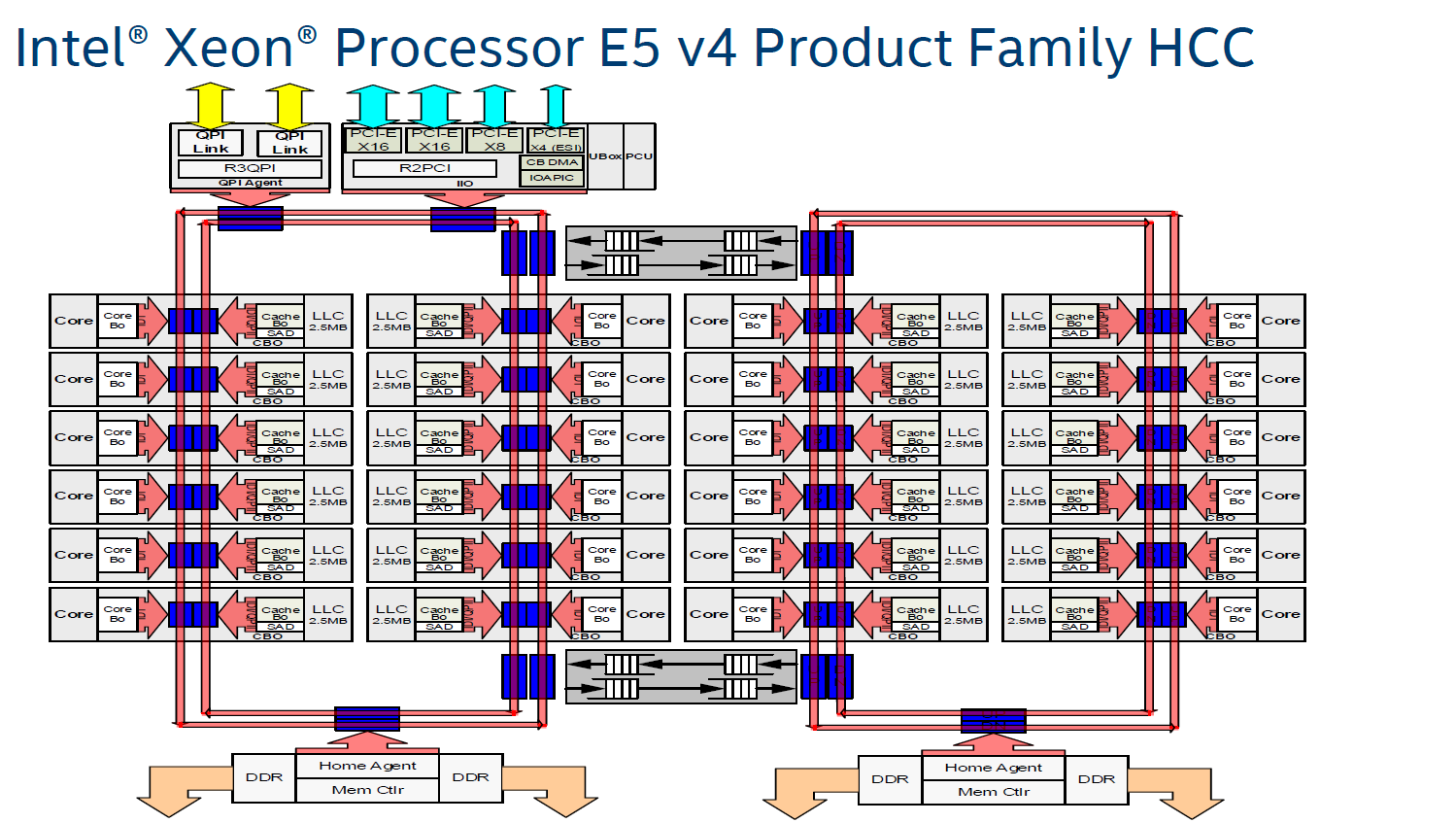
With Intel’s three-die program on its enterprise chips, each one used different variants of the ring bus topology. On Broadwell-E, the 10-core LCC design used a single ring bus for all 8 cores and the DRAM controller/PCIe root complex, whereas the HCC and XCC designs both had dual ring buses that used router communication methods to talk between each other. Now obviously talking to a core on the other ring bus added latency, and was sometimes considered a ‘non-uniform memory access’ (NUMA) environment on chip, with extra latency if you needed data from memory on the other ring bus. (Typically NUMA is applied to dual socket platforms, where the DRAM on the other chip has a large delay.) Intel emphasized that the Broadwell-E design was memory location aware, and tried to keep relevant data local to the core it was needed on.
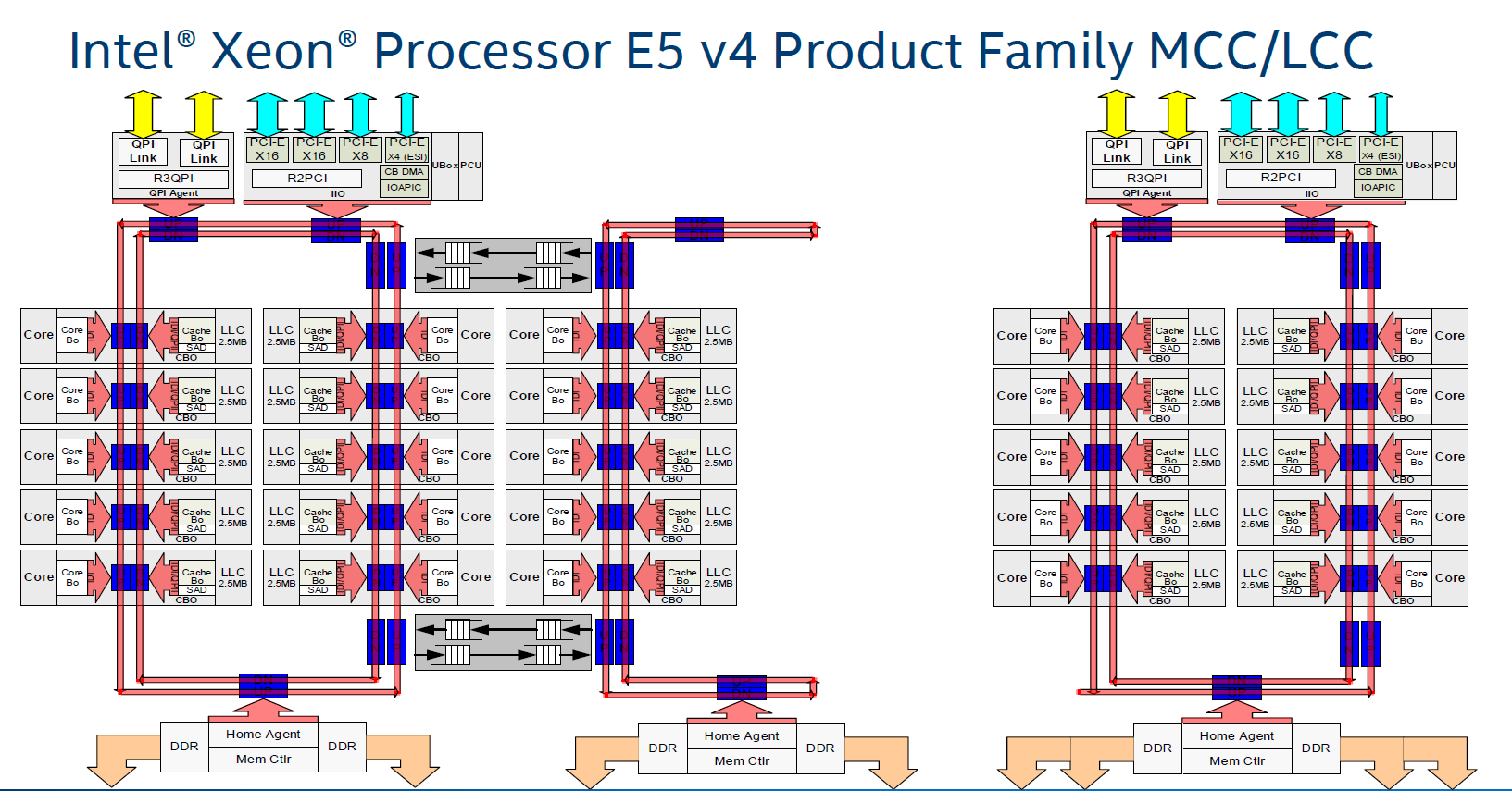
With the larger XCC CPUs for Broadwell-E, the ring buses become quite cumbersome: you end up with one ring bus servicing 12 cores, and another ring bus servicing 12 cores (due to the layout with other elements of the chip).
As more and more cores get added, what is the solution? More ring buses? How about a 2D array of ring buses? Or even a mesh or a network?

The announcement that Intel made in the past week was that Skylake-SP processors will use a mesh topology, whereby each CPU in the design will be connected to the ones above, below, and to the side. Earlier in the week I mentioned on Twitter that a mesh in this context, or as drawn above, is just an array of ring buses in a 2D arrangement, although new information has come to light.
There are several things to talk about the mesh here, so in no particular order:
Mesh Me Up
Intel already sells chips with mesh connectivity: the latest Xeon Phi Knights Landing many-core processors. These massive (~646mm2) chips have 72 cores arranged as 36 pairs, six memory channels and 16GB of MCDRAM, and using a ring bus (or a succession of ring buses) is probably not feasible.
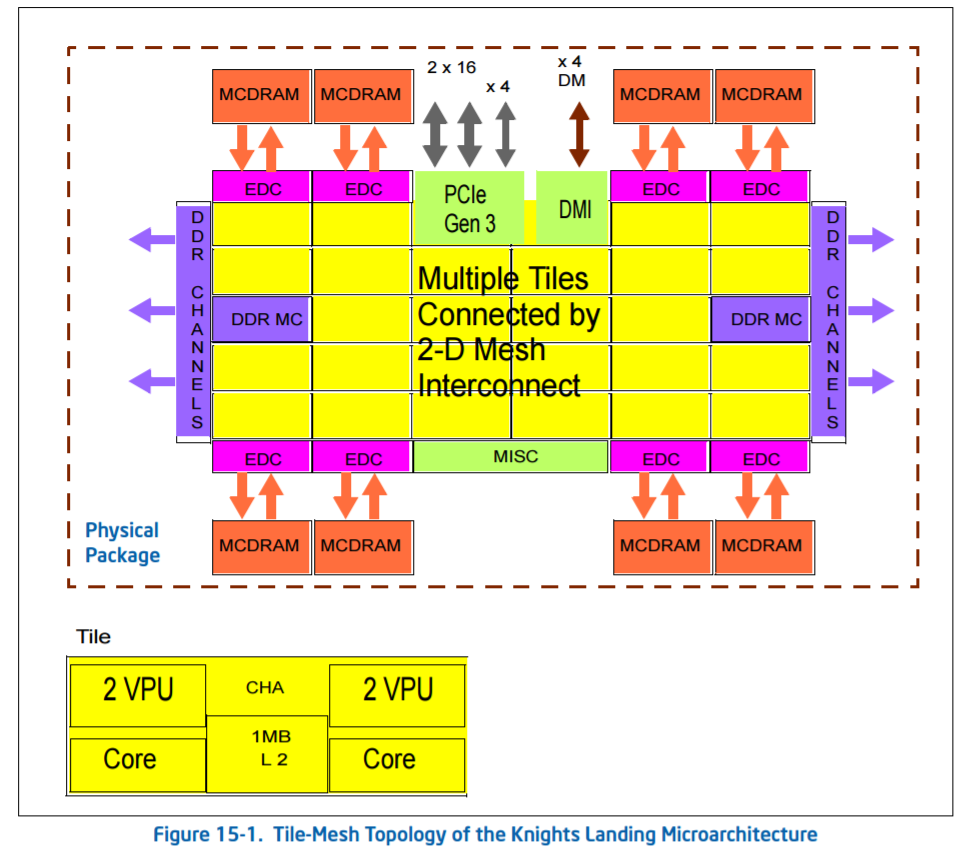
For KNL, Intel calls the mesh the ‘untile’. Taken from the KNL optimization guide:
‘At each mesh stop, there is a connection to the tile and a tag directory that identifies which L2 cache (if any) holds a particular cache line. [In Knights Landing] there is no shared L3 cache within a physical package, [so] memory accesses that miss in the tile must go over the mesh to the tag directory to identify any cached copies in another tile. Cache coherence uses the MESIF protocol. If the cache line is not cached in another tile, then a request goes to memory.’
Knights Landing can run in a variety of mesh modes, due to the lack of an L3 but the presence of an intermediary MCDRAM layer, certain modes to do with the memory hierarchy help with different codes. It is not known if Skylake-SP will have the same feature set.
When distributing cores along a mesh, another way to think about it is as a big routing environment. There are two ways – each core could talk to a central processing router which then sends information as it is needed, or each core acts as a networking point itself, forwarding packets in the direction it is needed. The first method, commonly known as a crossbar method, is easier to implement but can be bottlenecked very easily, not to mention power hungry if the whole crossbar needs to be enabled all the time. The second method, where every core is a router node, looks like what we have already in the image Intel provided.
The announcement Intel made was done officially by Dr Akhilesh Kumar, one of Skylake-SP’s CPU architects. He has been at Intel for a number of years, and digging back through releases with his name on popped up a very interesting paper regarding how to implement a router-like mesh in a multi-core environment, published in March 2014 which is about the right time when Skylake-SPs mesh was being developed. We haven’t had confirmation from Intel that this is how Skylake-SP’s mesh is actually like, though it is worth covering what is in the paper.
For anyone interested, the paper is called MoDe-X: Microarchitecture of a Layout-Aware Modular Decoupled Crossbar for On-Chip Interconnects, IEEE Transactions on Computers, Vol. 63, No. 3, March 2014 P622.
MoDe-X: Is This Skylake-SP’s Mesh?
As mentioned above, the easiest way for a mesh/router is through a crossbar. When the design instead uses each core as a node in the mesh, the result is essentially a ‘mini’ decoupled crossbar in each core acting as the director for data coming in and out of the core. With each core in control of its own actions, the design becomes modular. Put these elements together, and you have a MOdular DEcoupled Crossbar, or MoDe-X.
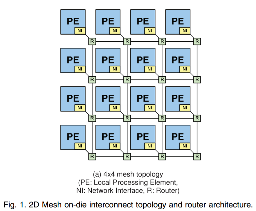
Each core has an integrated network interface and a router, with each router connected to the four routers around it (or 2 routers for corners and 3 routers for edges). A data packet can come in one of five directions – north, south, east, west, or from the core the router is attached to. The data packet then needs to be sent to one of five directions again: north, south, east, west, or to the core the router is attached to. If each core is essentially a node on a 2D map with an x-ordinate and a y-ordinate, if a packet needs to go to (0,0), the router can send it on its way as it knows which nodes are nearest to it. There are algorithms designed to reduce congestion, such as only moving in the x-direction until you are correct then start moving in the y-direction, but a basic system will have buffers and queues and will know how busy the local network congestion is.
The default way to design the router is to take the date from every input, decided where to send it, then send it. The MoDe-X design does it a little differently, and essentially splits the directions up into three groups: one group is north/south, one group is east/west, and the local core is the third group. The following diagram is a bit complex, but we’ll go through it:
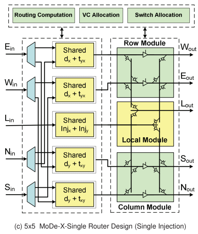
On the left are the five inputs: E, W, L (local), N, S.
On the right are the five outputs, W, E, L, S, N
The first column of ‘shared’ boxes determines where the data wants to go: does it need to traverse a row, a column, or stay local. From each input, there are only two arrows going to either the top pair or the bottom pair of ‘shared’ boxes. Depending on contention and allocation, the data is then sent to the second column whereby if the data needed to change columns, it could either go to Sout or Nout and if it needed to change rows into Wout or Eout. In both circumstances the data could go to the local node.
In the research paper, there is a six-input design which modifies the local input in order to make the wiring in the second half of the design easier (and it lowers power), but the image above is a fair representation of the idea. There are other additions in the paper as well, with layout aware arrangements (how exactly you put it together in silicon) as well as feeder wires such that if data needs to continue in the same direction it can do so with less effort.
The paper is very dense (it took me a while to get to grips with it), but worth a read if you are interested. I found it easier to consider it more like a router, than an on-chip mesh. As mentioned, this is a 2014 paper, and shows simulation data on an 8x8 grid of cores, where this design is both lower power and smaller area than a generic mesh design or competing designs. There were some areas where the generic design had marginally better latency, but the power conservation numbers (due to the wiring reduction and an aggressive power gating scheme to disable certain parts for up to 99% less power use) makes it a more attractive option (especially in multi-core CPUs). Intel was doing simulation work in early 2014 (which means 2013), and the paper mentions that they were in the process of putting these ideas into silicon. It wouldn’t be too far-fetched to consider that this is what we are seeing today.


264 Comments
View All Comments
Soheil - Sunday, June 25, 2017 - link
Anyone knows why 1600X better than 1800X?OddFriendship8989 - Thursday, June 29, 2017 - link
I'm late here as usual but why are you not comparing against the 7700k and 7600k? I get that these are HEDT chips, but it's worth comparing against the high end mainstream especially when the 7800x and 7700k are priced similarly that someone MIGHT consider jumping over.I hate to say it but this is the typical stuff you guys used to do, and I know it takes more time to put together more CPUs, but logical comparisons MUST be made and these charts show a bit of laziness.
ashlol - Friday, June 30, 2017 - link
can we have the GPU tests pleaseOxford Guy - Saturday, July 1, 2017 - link
"The discussion on whether Intel should be offering a standard goopy TIM or the indium-tin solder that they used to (and AMD uses) is one I’ve run on AnandTech before, but there’s a really good guide from Roman Hartung, who overclocks by the name der8auer. I’m trying to get him to agree to post it on AnandTech with SKL-X updates so we can discuss it here, but it really is some nice research. You can find the guide over at http://overclocking.guide."If you have a point to make then make it. After all, you said you've already "run" this discussion before. Tell us why polymer TIM is a better choice than solder (preferably without citing cracks from liquid nitrogen cooling).
ashlol - Monday, July 3, 2017 - link
Anyway both are bad since you have to delid it to achieve good cooling. I have delidded a 4770k and a 6700k and put liquid metal TIM between the die and the IHS and they both run 15°C cooler at 4.6-4.7GHz@60°C with custom loop. And from seeing the temperature under overclock I will have to delid those skylake-x too.parlinone - Tuesday, July 4, 2017 - link
What I find most shocking is a $329 Ryzen 1700 outperforms a $389 7800X at Cinebench...for less than half the power.The performance to power ratio translates to 239% in AMD's advantage. That's unprecedented, and I never imagined to see that day.
dwade123 - Thursday, July 6, 2017 - link
Only in Cinebench and AES is where Ryzen look good. 7800x beats the 1800x in everything else in this review. Ryzen is too inconsistent in both productivity and gaming. It is priced accordingly to that and not out of good faith from AMD. This is also the reason why Coffee Lake will only top out at 6 cores. because it can consistently beat the best Ryzen model.IGTrading - Friday, July 14, 2017 - link
I absolutely disagree with the conclusion. The correct conclusion can only drawn when comparin apples to apples. Oh, if you want to be objective and compare apples to oranges, you can't just take into considerantion today's benchmark results and price. Have we forgotten about the days we REVIEWERS were complaining about the high power consumption of Pentium 4 and Pentium D ?! What about the FX 8350 ?! Is power consumption not an objective metric anymore?! What about platform price ?! What about price/performance?! Why do some people get suddenly blinded by marketing money?! Conclusion: i-7900X is the highest performance the home power user can get today if money for the CPU , mobo and subsequent power consumption are not an issue. Comparing apples to apples or core for core, the i7820X clearly shows Intel's anxiety with Zen. The i7820X consumes 40% more than the AMD 1800X and costs 20% more while its motherboard is 200% the price. So paying all these heaps of money, CORE for CORE the Intel 7820X is a bit faster in some benchmarks, as it should be considering the power consumption and price you pay, EQUAL in a few benchmarks and SLOWER in a few other benchmarks. Would you pay the serious extra money for this ?! And put up with the 40% higher power consumption and heat generation ?! Come ooooon ...azulon1 - Sunday, July 16, 2017 - link
Wow how exactly is this fair that Intel gets a pass for gaming, because there were problems with the problem with the platform. If I remember Rison also had a problem with gaming. But it didn’t stop you guys then did it. don’t group me into AMD fanboy, But why such a bais?Soheil - Saturday, July 29, 2017 - link
no one answer to me? why 1600X better than 1700 and 1700X and some time better than 1800X?what about 1600? is good like as 1600X for gaming or not?