HiSilicon Kirin 960: A Closer Look at Performance and Power
by Matt Humrick on March 14, 2017 7:00 AM EST- Posted in
- Smartphones
- Mobile
- SoCs
- HiSilicon
- Cortex A73
- Kirin 960
HiSilicon’s Kirin 950 proved to be a breakout product for the Huawei subsidiary, ultimately finding a home in many of Huawei’s flagship phones, including the Mate 8, P9, P9 Plus, and Honor 8. Its big.LITTLE combination of four A72 and four A53 CPU cores manufactured on TSMC’s 16nm FF+ FinFET process delivered excellent performance and efficiency. Somewhat surprisingly, it turned out to be one of the best, if not the best, implementation of ARM’s IP we’ve seen.
Because of the 950’s success, we were eager to see what improvements the Kirin 960 could offer. In our review of the Huawei Mate 9, the first device to use the new SoC, we saw gains in most of our performance and battery life tests relative to the Mate 8 and its Kirin 950 SoC. Now it’s time to dive a little deeper and answer some of our remaining questions: How does IPC compare between the A73, A72, and other CPU cores? How is memory performance impacted by the A73’s microarchitecture changes? Does CPU efficiency improve? How much more power do the extra GPU cores consume?
| HiSilicon High-End Kirin SoC Lineup | |||
| SoC | Kirin 960 | Kirin 955 | Kirin 950 |
| CPU | 4x Cortex-A73 @ 2.36GHz 4x Cortex-A53 @ 1.84GHz |
4x Cortex-A72 @ 2.52GHz 4x Cortex-A53 @ 1.81GHz |
4x Cortex-A72 @ 2.30GHz 4x Cortex-A53 @ 1.81GHz |
| GPU | ARM Mali-G71MP8 1037MHz |
ARM Mali-T880MP4 900MHz |
|
| Memory | 2x 32-bit LPDDR4 @ 1866MHz 29.9GB/s |
2x 32-bit LPDDR3 @ 933MHz (14.9GB/s) or 2x 32-bit LPDDR4 @ 1333MHz (21.3GB/s) (hybrid controller) |
|
| Interconnect | ARM CCI-550 | ARM CCI-400 | |
| Storage | UFS 2.1 | eMMC 5.0 | |
| ISP/Camera | Dual 14-bit ISP (Improved) |
Dual 14-bit ISP 940MP/s |
|
| Encode/Decode | 2160p30 HEVC & H.264 Decode & Encode 2160p60 HEVC Decode |
1080p H.264 Decode & Encode 2160p30 HEVC Decode |
|
| Integrated Modem | Kirin 960 Integrated LTE (Category 12/13) DL = 600Mbps 4x20MHz CA, 64-QAM UL = 150Mbps 2x20MHz CA, 64-QAM |
Balong Integrated LTE (Category 6) DL = 300Mbps 2x20MHz CA, 64-QAM UL = 50Mbps 1x20MHz CA, 16-QAM |
|
| Sensor Hub | i6 | i5 | |
| Mfc. Process | TSMC 16nm FFC | TSMC 16nm FF+ | |
The Kirin 960 is the first SoC to use ARM’s latest A73 CPU cores, which seems fitting considering the Kirin 950 was the first to use ARM’s A72. Its CPU core frequencies see a negligible increase relative to the Kirin 950: 1.81GHz to 1.84GHz for the four A53s and 2.30GHz to 2.36GHz for the four A73s. Setting the peak operating point for the A73 cores lower than the 2.52GHz used by Kirin 955’s A72 cores, and lower still than the 2.8GHz that ARM targets for 16nm, is an interesting and deliberate choice by HiSilicon to limit the CPU’s power envelope, allowing the bigger GPU to take a larger chunk.
We’ve already discussed the A73’s microarchitecture in depth, so I’ll just summarize a few of the highlights. For starters, the A73 stems from the A17 and does not belong to the A15/A57/A72 Austin family tree. This means the differences between the A72 and A73 are more substantial than the small change in product numbering would suggest, particularly in the CPU’s front end.
The biggest difference is a reduction in decoder width, which is now 2-wide instead of 3-wide like the A72. This sounds like a downgrade on paper; however, there’s likely some workloads where the A72’s instruction fetch block fails to consistently saturate the decoder, so the actual performance impact of the A73’s narrower decode stage may not be that severe.
In many cases, instruction dispatch throughput should actually improve relative to the A72. The A73’s shorter pipeline reduces front-end latency, including 1-2 fewer cycles for the decoder, which can decode most instructions in a single cycle, and 1 less cycle for the fetch stage. The L1 instruction cache doubles in size and is optimized for better throughput, and changes to the instruction fetch block reduce instruction bubbles. ARM also says the A73 includes a new, more accurate branch predictor, with a larger BTAC (Branch Target Address Cache) structure and a new 64-entry “micro-BTAC” for accelerating branch prediction.
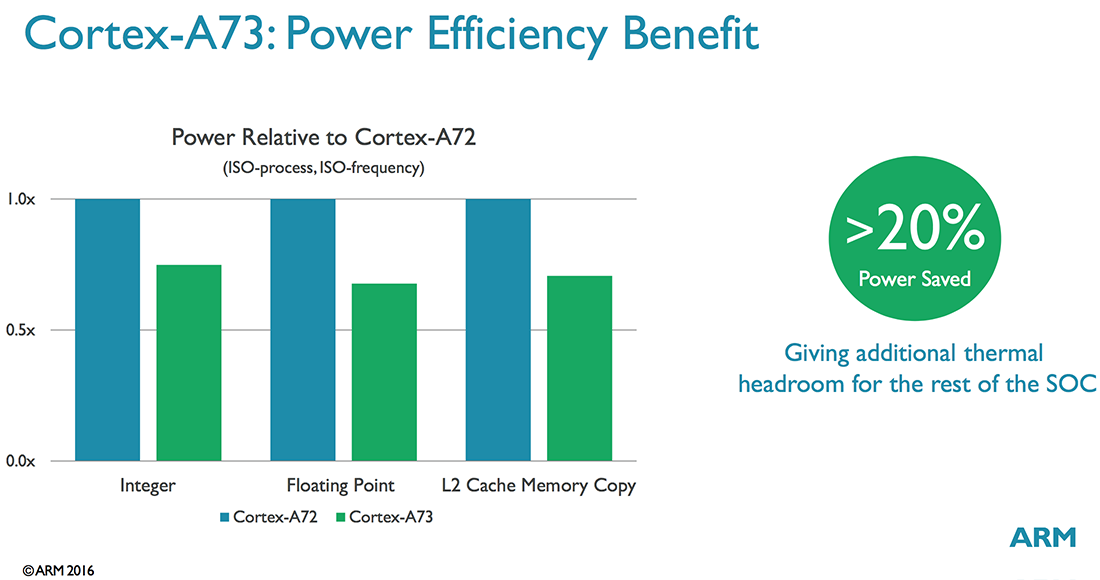
There are several other changes to the front end too, not to mention further along the pipeline, but it should be obvious by now that the A73 is a very different beast than the A72, grown from a different design philosophy. While the Austin family (A72) targeted industrial and low-power server applications in addition to mobile, the A73 focuses specifically on mobile, where power and area become an even higher priority. ARM says the A73 consumes 20%-30% less power than the A72 (same process, same frequency) and is up to 25% smaller (same process, same performance targets).
When it comes to Kirin 960’s GPU, however, HiSilicon is clearly chasing performance instead of efficiency. With its previous SoCs, the Kirin 950/955 in particular, HiSilicon was criticized for using four-core Mali configurations while Samsung packed in eight or twelve Mali cores in its Exynos SoCs and Qualcomm squeezed more ALU resources into its Adreno GPUs. This was not entirely justified, though, because the Kirin 950’s Mali-T880MP4 GPU was capable of playing nearly any game available at acceptable frame rates and the performance difference between the Mate 8 (Kirin 950), Samsung Galaxy S7 edge (Snapdragon 820), and Galaxy S7 (Exynos 8890) after reaching thermal equilibrium is minimal.
Whether in response to this criticism or to enable future use cases such as VR/AR, HiSilicon has significantly increased the Kirin 960’s peak GPU performance. Not only is it the first to use ARM’s latest Mali-G71 GPU, but it doubles core count to eight and boosts the peak frequency to 1037MHz, 15% higher than the 950’s smaller GPU.
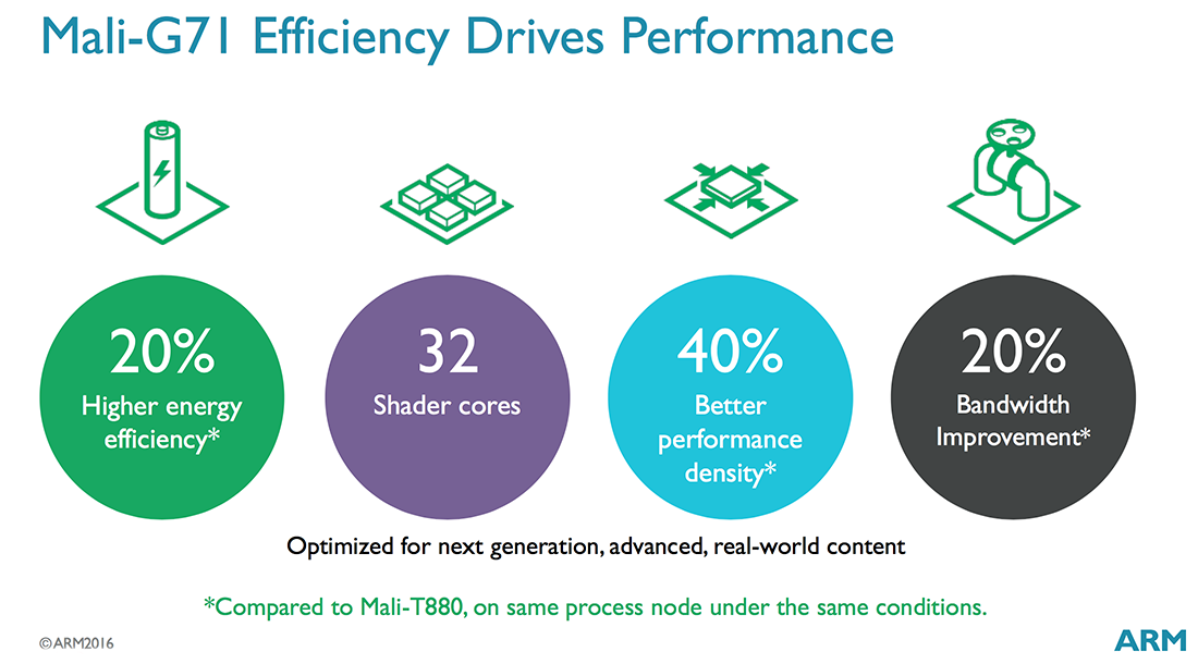
The Mali-G71 uses ARM’s new Bifrost microarchitecture, which moves from an SIMD ISA that relied on Instruction Level Parallelism (ILP) to a scalar ISA designed to take advantage of Thread Level Parallelism (TLP) like modern desktop GPU architectures from Nvidia and AMD. I’m not going to explain the difference in depth here, but basically this change allows better utilization of the shader cores, increasing throughput and performance. ARM’s previous Midgard microarchitecture needed to extract 4 instructions from a single thread and execute them concurrently to achieve full utilization of a single shader core, which is not easy to do consistently. In contrast, Bifrost can group 4 separate threads together on a shader core and execute a single instruction from each one, which is more inline with modern graphics and compute workloads.
Now that we have a better understanding for Kirin 960’s design goals—better efficiency for the CPU and higher peak performance for the GPU—and a summary of the hardware changes HiSilicon made to achieve them, we’re ready to see how the performance and power consumption of the Kirin 960 compares to the 950/955 and other recent SoCs.


86 Comments
View All Comments
Meteor2 - Wednesday, March 15, 2017 - link
Andrei! That's a pretty big stamp :). I hope you're well.aryonoco - Tuesday, March 14, 2017 - link
A great article, very insightful, and absolutely unique on the web.Well done Matt, well done AT.
name99 - Tuesday, March 14, 2017 - link
One issue in comparing the GeekBench results to the SPEC results is the question of compiler optimization.Were the SPEC results specifically targeted at the A73? And using the most recent version of LLVM?
GeekBench (as far as I can tell) compiles a particular version (say version 4) with a particular compiler and target, and does not update those over time until say GeekBench 5 is released. This is not an awful practice --- it certainly makes it a lot easier to compare results in such a way that compiler optimizations don't confuse the issue. But it DOES mean that
- the SPEC results may be picking up A73 specific tuning that GeekBench does not reflect.
- depending on when you compiled the comparison AArch64 binaries, some fraction (and this may be high, 5% or more) of the A73 "improvement" may reflect LLVM improvement, both generally and in specific ARMv8 optimizations.
If the SPEC results were "maximally" compiled (so that LTO was used, something that only really started to work well in the most recent LLVM versions) there could be even more of a compiler-based discrepancy.
MrSewerPickle - Thursday, March 16, 2017 - link
Thank you guys for the review. Please keep these details up and going. You guys are a rarity these days and still doing great. Facts are hard to post without rambling about them and excessive opinion rambling accompanying it.socalbigmike - Thursday, March 16, 2017 - link
Just don't try and run any apps on it! Because half of them will NOT run.darkich - Thursday, March 23, 2017 - link
Wow they messed up again with that high clocked GPU implementation. Just ridiculous..Huweai making the same mistake over and over again, refusing to take note from Samsung ..I'm certain the Samsung's low clocked G71 MP18 will consume far less power than this 8 core setup!