AMD Zen Microarchitecture: Dual Schedulers, Micro-Op Cache and Memory Hierarchy Revealed
by Ian Cutress on August 18, 2016 9:00 AM ESTDeciphering the New Cache Hierarchy
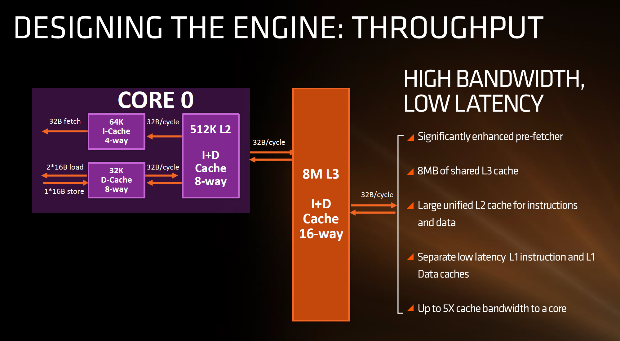
The cache hierarchy is a significant deviation from recent previous AMD designs, and most likely to its advantage. The L1 data cache is both double in size and increased in associativity compared to Bulldozer, as well as being write-back rather than write-through. It also uses an asymmetric load/store implementation, identifying that loads happen more often than stores in the critical paths of most work flows. The instruction cache is no longer shared between two cores as well as doubling in associativity, which should decrease the proportion of cache misses. AMD states that both the L1-D and L1-I are low latency, with details to come.
The L2 cache sits at half a megabyte per core with 8-way associativity, which is double that of Intel’s Skylake which has 256 KB/core and is only 4-way. On the other hand, Intel’s L3/LLC on their high-end Skylake SKUs is at 2 MB/core or 8 MB/CPU, whereas Zen will feature 1 MB/core and both are at 16-way associativity.
Edit 7:18am: Actually, the slide above is being slightly evasive in its description. It doesn't say how many cores the L3 cache is stretched over, or if there is a common LLC between all cores in the chip. However, we have recieved information from a source (which can't be confirmed via public AMD documents) that states that Zen will feature two sets of 8MB L3 cache between two groups of four cores each, giving 16 MB of L3 total. This would means 2 MB/core, but it also implies that there is no last-level unified cache in silicon across all cores, which Intel has. The reasons behind something like this is typically to do with modularity, and being able to scale a core design from low core counts to high core counts. But it would still leave a Zen core with the same L3 cache per core as Intel.
| Cache Levels | ||||
| Bulldozer FX-8150 |
Zen | Broadwell-E i7-6950X |
Skylake i7-6700K |
|
| L1 Instruction | 64 KB 2-way per module |
64 KB 4-way | 32 KB 8-way | 32 KB 8-way |
| L1 Data | 16 KB 4-way Write Through |
32 KB 8-way Write Back |
32 KB 8-way Write-Back |
32 KB 8-way Write-Back |
| L2 | 2 MB 16-way per module |
512 KB 8-way | 256 KB 8-way | 256 KB 4-way |
| L3 | 1 MB/core 64-way |
1 or 2 MB/core ? 16-way |
2.5 MB/core 16/20-way |
2 MB/core 16-way |
What this means, between the L2 and the L3, is that AMD is putting more lower level cache nearer the core than Intel, and as it is low level it becomes separate to each core which can potentially improve single thread performance. The downside of bigger and lower (but separate) caches is how each of the cores will perform snoop in each other’s large caches to ensure clean data is being passed around and that old data in L3 is not out-of-date. AMD’s big headline number overall is that Zen will offer up to 5x cache bandwidth to a core over previous designs.


216 Comments
View All Comments
Jleppard - Thursday, August 18, 2016 - link
OR the first to 5 GHzKevin G - Saturday, August 20, 2016 - link
IBM hit 5 Ghz back in 2008 with the POWER6.JlHADJOE - Sunday, August 21, 2016 - link
Given how quickly they were able to implement x86_64, my bet is Intel already thought about extending x86 to 64bits, they just didn't want to do it because they were pushing Itanium hard at the time.But then AMD comes out with AMD64, and (rather predictably) the market loves it, which puts a real damper on Intel's Itanium push and eventually they are forced to capitulate and follow suit.
hansmuff - Thursday, August 18, 2016 - link
Everyone copies success, what's new?bill.rookard - Thursday, August 18, 2016 - link
Well, it's not a complete copy. There are some difference which should make it interesting to see how the chips line up against each other. x2 L2 cache on Zen vs x2 L3 cache on Intel, the larger core/thread counts (let's hope they offer the 8c/16t to consumers), and of course, the big one being how this all affects the integrated graphics in APU form.Will the change to 16nm FinFET allow them to put in more GPU? What kind of clocks and/or power envelope will this run at? A lot of this makes a huge difference in the types of systems which can be made - a powerful hex-core CPU with a beefier IGP in a 60-80w TDP would be nice to see.
smilingcrow - Thursday, August 18, 2016 - link
There is definitely gong to be a consumer 8c/16t chip.Ian Cutress - Thursday, August 18, 2016 - link
The 8c will be coming to consumers in the AM4 chipset in Q1. :)Flunk - Thursday, August 18, 2016 - link
I wonder what the resale value of my 6700K and Z170 board will be in Q1 ;).Morawka - Thursday, August 18, 2016 - link
you'll get more cores but not more IPC. all signs point to skylake being at least 2 years ahead of zen, although since intel has barely increased performance in 2 years, it shouldnt make to big of a difference, in gaming at least.tamalero - Friday, August 19, 2016 - link
Disagree, the performance boost of each generation is always less than 5% in the last designs by intel.Only a few tests show really higher performance per clock.