AMD Zen Microarchitecture: Dual Schedulers, Micro-Op Cache and Memory Hierarchy Revealed
by Ian Cutress on August 18, 2016 9:00 AM ESTLow Power, FinFET and Clock Gating
When AMD launched Carrizo and Bristol Ridge for notebooks, one of the big stories was how AMD had implemented a number of techniques to improve power consumption and subsequently increase efficiency. A number of those lessons have come through with Zen, as well as a few new aspects in play due to the lithography.
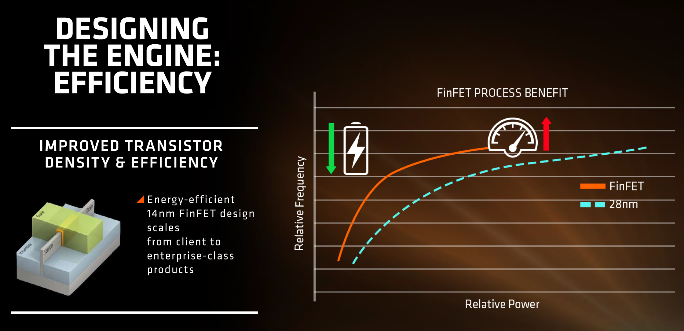
First up is the FinFET effect. Regular readers of AnandTech and those that follow the industry will already be bored to death with FinFET, but the design allows for a lower power version of a transistor at a given frequency. Now of course everyone using FinFET can have a different implementation which gives specific power/performance characteristics, but Zen on the 14nm FinFET process at Global Foundries is already a known quantity with AMD’s Polaris GPUs which are built similarly. The combination of FinFET with the fact that AMD confirmed that they will be using the density-optimised version of 14nm FinFET (which will allow for smaller die sizes and more reasonable efficiency points) also contributes to a shift of either higher performance at the same power or the same performance at lower power.
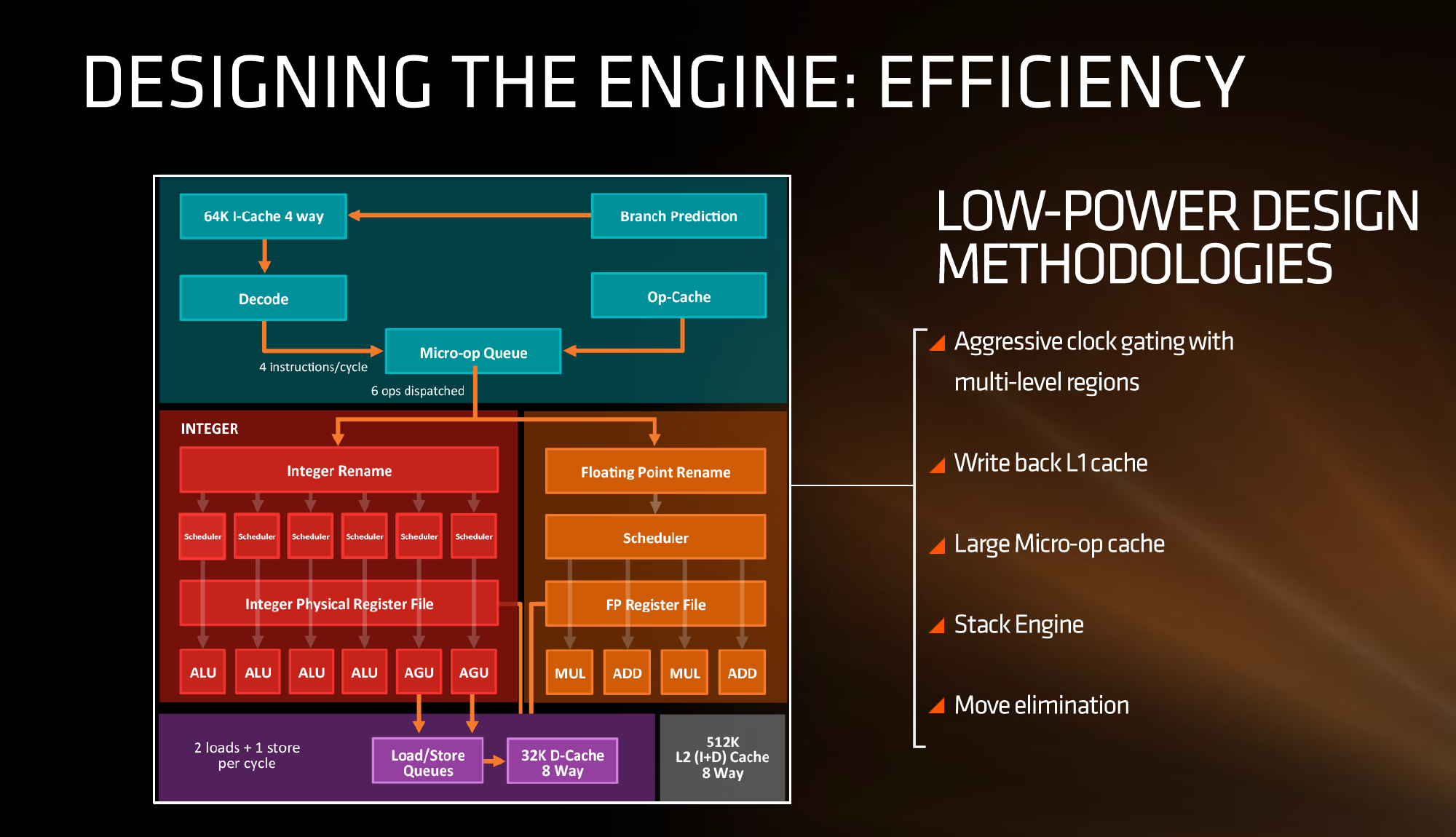
AMD stated in the brief that power consumption and efficiency was constantly drilled into the engineers, and as explained in previous briefings, there ends up being a tradeoff between performance and efficiency about what can be done for a number of elements of the core (e.g. 1% performance might cost 2% efficiency). For Zen, the micro-op cache will save power by not having to go further out to get instruction data, improved prefetch and a couple of other features such as move elimination will also reduce the work, but AMD also states that cores will be aggressively clock gated to improve efficiency.
We saw with AMD’s 7th Gen APUs that power gating was also a target with that design, especially when remaining at the best efficiency point (given specific performance) is usually the best policy. The way the diagram above is laid out would seem to suggest that different parts of the core could independently be clock gated depending on use (e.g. decode vs FP ports), although we were not able to confirm if this is the case. It also relies on having very quick (1-2 cycle) clock gating implementations, and note that clock gating is different to power-gating, which is harder to implement.


216 Comments
View All Comments
jamyryals - Monday, August 22, 2016 - link
Excited to see if they execute, I'm rooting for AMD. After two straight Intel chips, I'd love to spend money with AMD again.slyronit - Tuesday, August 23, 2016 - link
I would be happy to see AMD succeed and be relevant in the desktop/tablet/laptop space again. I have stuck with AMD over the years because of the low price to performance ratio and good multithread performance (I use photo editing apps which multithread well) and because Intel is a mis-leading, monopolistic company.soulLover - Thursday, August 25, 2016 - link
no avx2 ? After excluding the Micro-OP cache, the four instruction per cycle are to feed 2 x 128 bit, right ? i.e. 4 x 64 bits / cycle. If I'm not wrong AMD is lacking serious parallelism in SIMD than Intel AVX2.unimatrix725 - Sunday, August 28, 2016 - link
I have read both In depth Zen reviews, however something huge is missing! No one or any tech site that I'm aware of has went in depth about Global Memory Interface. The best I got out of it was a variant of a PPC on Wikipedia? There needs to be coverage of this. I believe it critical to Zen & AM4 in general. Since there is no more NB&ORSB. Shocked not even Wikipedia has an article. A double edge sword more or less...patrickjchase - Sunday, August 28, 2016 - link
The comment that "some put [a micro-op cache] as a major stepping stone for Conroe" is wrong on a couple levels:First, Conroe didn't have a uop cache. Like many other micro-architectures before and since it could use its uop queue to buffer small loops, but had no uop cache as such.
Second, Intel cores had uop caches long before Conroe. The first Intel x86 microarchitecture with a first-level I-cache that stored decoded uops was Pentium-4. The oft-maligned trace cache was in fact a uop cache. The fact that it went a step beyond and stored superblocks of decoded uops doesn't change the fact that it was a uop cache.
The uop caches first appeared in the "non-Pentium-4" Intel x86 line in Sandy Bridge, two full tocks after Conroe.
Hixbot - Friday, September 2, 2016 - link
Any chance Zen competition will push Intel to release an 8-core mainstream CPU for about $300?