AMD Zen Microarchitecture: Dual Schedulers, Micro-Op Cache and Memory Hierarchy Revealed
by Ian Cutress on August 18, 2016 9:00 AM ESTDeciphering the New Cache Hierarchy
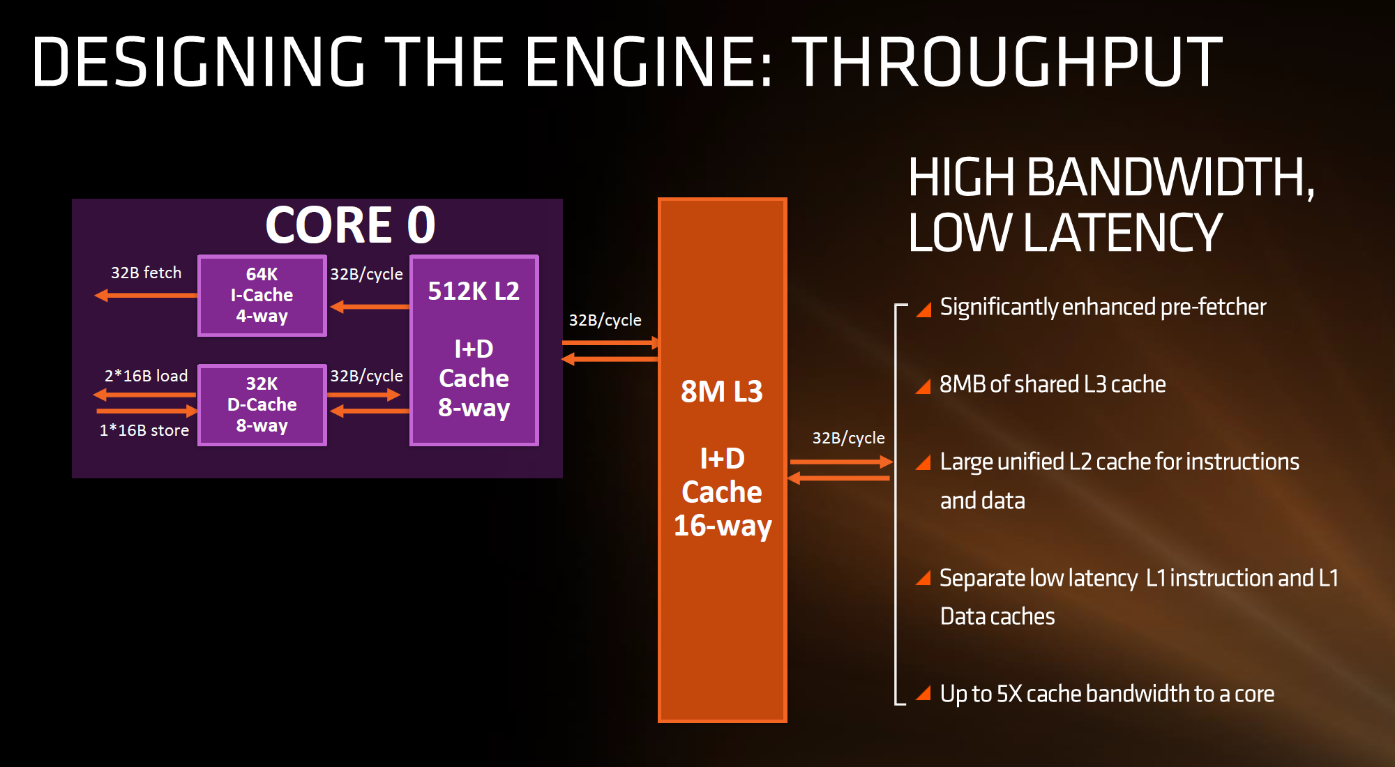
The cache hierarchy is a significant deviation from recent previous AMD designs, and most likely to its advantage. The L1 data cache is both double in size and increased in associativity compared to Bulldozer, as well as being write-back rather than write-through. It also uses an asymmetric load/store implementation, identifying that loads happen more often than stores in the critical paths of most work flows. The instruction cache is no longer shared between two cores as well as doubling in associativity, which should decrease the proportion of cache misses. AMD states that both the L1-D and L1-I are low latency, with details to come.
The L2 cache sits at half a megabyte per core with 8-way associativity, which is double that of Intel’s Skylake which has 256 KB/core and is only 4-way. On the other hand, Intel’s L3/LLC on their high-end Skylake SKUs is at 2 MB/core or 8 MB/CPU, whereas Zen will feature 1 MB/core and both are at 16-way associativity.
Edit 7:18am: Actually, the slide above is being slightly evasive in its description. It doesn't say how many cores the L3 cache is stretched over, or if there is a common LLC between all cores in the chip. However, we have recieved information from a source (which can't be confirmed via public AMD documents) that states that Zen will feature two sets of 8MB L3 cache between two groups of four cores each, giving 16 MB of L3 total. This would means 2 MB/core, but it also implies that there is no last-level unified cache in silicon across all cores, which Intel has. The reasons behind something like this is typically to do with modularity, and being able to scale a core design from low core counts to high core counts. But it would still leave a Zen core with the same L3 cache per core as Intel.
| Cache Levels | ||||
| Bulldozer FX-8150 |
Zen | Broadwell-E i7-6950X |
Skylake i7-6700K |
|
| L1 Instruction | 64 KB 2-way per module |
64 KB 4-way | 32 KB 8-way | 32 KB 8-way |
| L1 Data | 16 KB 4-way Write Through |
32 KB 8-way Write Back |
32 KB 8-way Write-Back |
32 KB 8-way Write-Back |
| L2 | 2 MB 16-way per module |
512 KB 8-way | 256 KB 8-way | 256 KB 4-way |
| L3 | 1 MB/core 64-way |
1 or 2 MB/core ? 16-way |
2.5 MB/core 16/20-way |
2 MB/core 16-way |
What this means, between the L2 and the L3, is that AMD is putting more lower level cache nearer the core than Intel, and as it is low level it becomes separate to each core which can potentially improve single thread performance. The downside of bigger and lower (but separate) caches is how each of the cores will perform snoop in each other’s large caches to ensure clean data is being passed around and that old data in L3 is not out-of-date. AMD’s big headline number overall is that Zen will offer up to 5x cache bandwidth to a core over previous designs.


216 Comments
View All Comments
jamyryals - Monday, August 22, 2016 - link
Excited to see if they execute, I'm rooting for AMD. After two straight Intel chips, I'd love to spend money with AMD again.slyronit - Tuesday, August 23, 2016 - link
I would be happy to see AMD succeed and be relevant in the desktop/tablet/laptop space again. I have stuck with AMD over the years because of the low price to performance ratio and good multithread performance (I use photo editing apps which multithread well) and because Intel is a mis-leading, monopolistic company.soulLover - Thursday, August 25, 2016 - link
no avx2 ? After excluding the Micro-OP cache, the four instruction per cycle are to feed 2 x 128 bit, right ? i.e. 4 x 64 bits / cycle. If I'm not wrong AMD is lacking serious parallelism in SIMD than Intel AVX2.unimatrix725 - Sunday, August 28, 2016 - link
I have read both In depth Zen reviews, however something huge is missing! No one or any tech site that I'm aware of has went in depth about Global Memory Interface. The best I got out of it was a variant of a PPC on Wikipedia? There needs to be coverage of this. I believe it critical to Zen & AM4 in general. Since there is no more NB&ORSB. Shocked not even Wikipedia has an article. A double edge sword more or less...patrickjchase - Sunday, August 28, 2016 - link
The comment that "some put [a micro-op cache] as a major stepping stone for Conroe" is wrong on a couple levels:First, Conroe didn't have a uop cache. Like many other micro-architectures before and since it could use its uop queue to buffer small loops, but had no uop cache as such.
Second, Intel cores had uop caches long before Conroe. The first Intel x86 microarchitecture with a first-level I-cache that stored decoded uops was Pentium-4. The oft-maligned trace cache was in fact a uop cache. The fact that it went a step beyond and stored superblocks of decoded uops doesn't change the fact that it was a uop cache.
The uop caches first appeared in the "non-Pentium-4" Intel x86 line in Sandy Bridge, two full tocks after Conroe.
Hixbot - Friday, September 2, 2016 - link
Any chance Zen competition will push Intel to release an 8-core mainstream CPU for about $300?