Hidden Secrets: Investigation Shows That NVIDIA GPUs Implement Tile Based Rasterization for Greater Efficiency
by Ryan Smith on August 1, 2016 5:00 AM EST
As someone who analyzes GPUs for a living, one of the more vexing things in my life has been NVIDIA’s Maxwell architecture. The company’s 28nm refresh offered a huge performance-per-watt increase for only a modest die size increase, essentially allowing NVIDIA to offer a full generation’s performance improvement without a corresponding manufacturing improvement. We’ve had architectural updates on the same node before, but never anything quite like Maxwell.
The vexing aspect to me has been that while NVIDIA shared some details about how they improved Maxwell’s efficiency over Kepler, they have never disclosed all of the major improvements under the hood. We know, for example, that Maxwell implemented a significantly altered SM structure that was easier to reach peak utilization on, and thanks to its partitioning wasted much less power on interconnects. We also know that NVIDIA significantly increased the L2 cache size and did a number of low-level (transistor level) optimizations to the design. But NVIDIA has also held back information – the technical advantages that are their secret sauce – so I’ve never had a complete picture of how Maxwell compares to Kepler.
For a while now, a number of people have suspected that one of the ingredients of that secret sauce was that NVIDIA had applied some mobile power efficiency technologies to Maxwell. It was, after all, their original mobile-first GPU architecture, and now we have some data to back that up. Friend of AnandTech and all around tech guru David Kanter of Real World Tech has gone digging through Maxwell/Pascal, and in an article & video published this morning, he outlines how he has uncovered very convincing evidence that NVIDIA implemented a tile based rendering system with Maxwell.
In short, by playing around with some DirectX code specifically designed to look at triangle rasterization, he has come up with some solid evidence that NVIDIA’s handling of tringles has significantly changed since Kepler, and that their current method of triangle handling is consistent with a tile based renderer.
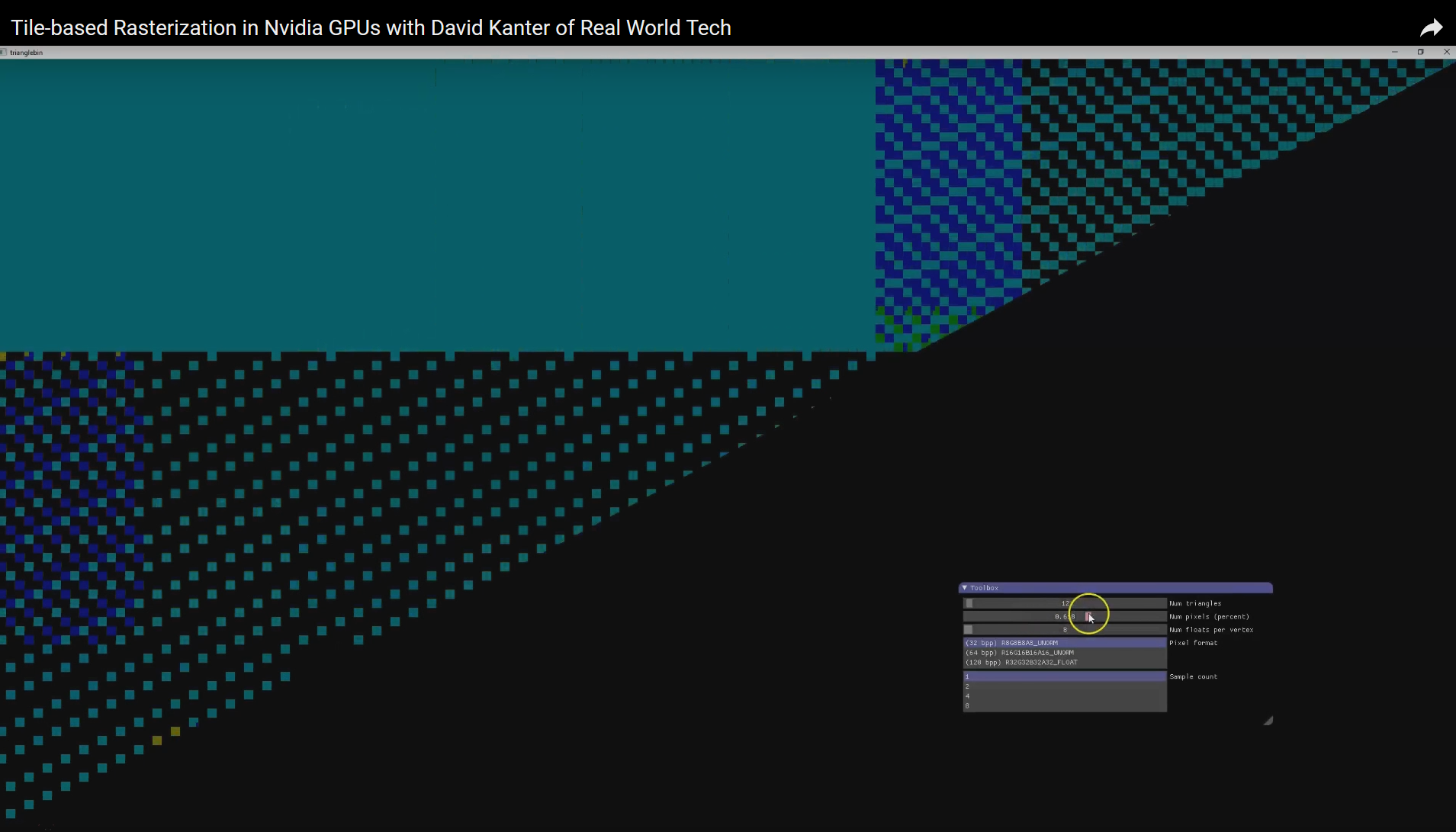
NVIDIA Maxwell Architecture Rasterization Tiling Pattern (Image Courtesy: Real World Tech)
Tile based rendering is something we’ve seen for some time in the mobile space, with both Imagination PowerVR and ARM Mali implementing it. The significance of tiling is that by splitting a scene up into tiles, tiles can be rasterized piece by piece by the GPU almost entirely on die, as opposed to the more memory (and power) intensive process of rasterizing the entire frame at once via immediate mode rendering. The trade-off with tiling, and why it’s a bit surprising to see it here, is that the PC legacy is immediate mode rendering, and this is still how most applications expect PC GPUs to work. So to implement tile based rasterization on Maxwell means that NVIDIA has found a practical means to overcome the drawbacks of the method and the potential compatibility issues.
In any case, Real Word Tech’s article goes into greater detail about what’s going on, so I won’t spoil it further. But with this information in hand, we now have a more complete picture of how Maxwell (and Pascal) work, and consequently how NVIDIA was able to improve over Kepler by so much. Finally, at this point in time Real World Tech believes that NVIDIA is the only PC GPU manufacturer to use tile based rasterization, which also helps to explain some of NVIDIA’s current advantages over Intel’s and AMD’s GPU architectures, and gives us an idea of what we may see them do in the future.
Source: Real World Tech


191 Comments
View All Comments
looncraz - Monday, August 1, 2016 - link
AMD was well ahead of nVidia in tessellation at one point. And, today, they are basically even (technically far ahead if you consider clock rates).Compare the RX 480 tessellation to the GTX 1060 tessellation:
AMD RX 480 Tessmark: 2240
NV GTX1060 Tessmark: 2269
And that RX480 is likely running at ~1.2Ghz, and the 1060 is running at ~1.8Ghz.
Scali - Monday, August 1, 2016 - link
Why would you look only at the clockspeed, the most meaningless spec of all?Let's look at the rest:
RX480:
Die size: 230 mm²
Process: GloFo 14 nm FinFET
Transistor count: 5.7 billion
TFLOPS: 5.1
Memory bandwidth: 256 GB/s
Memory bus: 256-bit
Memory size: 4/8 GB
TDP: 150W
GTX1060:
Die size: 200 mm²
Process: TSMC 16 nm FinFET
Transistor count: 4.4 billion
TFLOPS: 3.8
Memory bandwidth: 192 GB/s
Memory bus: 192-bit
Memory size: 6 GB
TDP: 120W
Pretty sad that the RX480 can only reach GTX1060 speeds, with higher specs all around (the memory interface is actually the same spec as GTX1070).
gamervivek - Monday, August 1, 2016 - link
If you're the same Scali, then I can see why they banned you from beyond3d.medi03 - Monday, August 1, 2016 - link
The only higher spec here is the die size.For number of transistors: that's the trade off. AMD packs more of them into the same area, but then runs them at lower clock.
Mem bandwidth is likely irrelevant.
Scali - Monday, August 1, 2016 - link
"Mem bandwidth is likely irrelevant."I wouldn't be too sure of that.
What Tessmark does is little more than displacement-mapping a simple sphere.
In a synthetic test like that, perhaps the bandwidth can affect the speed at which the displacementmap can be sampled, and therefore can have an effect on the total tessellation score.
It's an interesting area to explore by testing cards at different memory speeds, while leaving the GPU at the same clock.
TheJian - Tuesday, August 2, 2016 - link
You seem to be missing the point. Based on specs AMD should be leading this competition by >10%. Larger die, 1.3B extra transistors, 30 more watts, smaller process, 1.3TF extra, and far more bandwidth. Despite ALL of those specs leading on AMD's side, they LOSE to 1060 except in a few games they help fund to optimize (AOTS etc).https://www.reddit.com/r/nvidia/comments/4tyco0/th...
240 benchmarks over 51 games in a nice spreadsheet if you wanted it :)
findings:
On average, a 1060 is 13.72% better than a 480.
On average, when using DX11, a 1060 is 15.25% better than a 480.
On average, when using DX12, a 1060 is 1.02% worse than a 480.
On average, when using Vulkan, a 1060 is 27.13% better than a 480.
AMD won in 11.36% of DX11 titles, 71.43% of DX12 titles, and 50% of Vulkan titles.
The most commonly reviewed games were AotS, Hitman, RotTR, the Division, GTA V, and the Witcher 3.
Toss in a Doom fix coming soon (bethesda faq says pascal not working yet for async, hardocp verifies this showing older 1.08 libraries used instead of 1.0.11 or 1.0.17 etc) and surely NV finally concentrating on DX12 at some point, and you should get the picture. It's not going to get better for AMD who quit dx11 ages ago and moved to dx12/vulkan purely due to lack of funding for dx11 at the same time (and a hope we'd move to windows 10 while free...LOL). It's comic to me that people think AMD will win based on the games you can count on your hands, while NV is concentrating on where 99% of the games and users are (dx11/OpenGL/win7/win8 etc).
AMD gave up DX11 when Nvidia beat them in their own Mantle game test StarSwarm. Tested here and shown winning even at anandtech once NV concentrated on showing up mantle with dx11. AMD revenue and R&D tanked for the last 3-4yrs in a row, so should be no surprise to anyone how this is working out while they spend what little R&D they do have on chasing consoles instead of CORE products/drivers like NV decided to do. You can be sure Vega/ZEN would both be here ages ago if they hadn't chase xbox1/ps4 and now their new replacements coming soon yet again. They are both late due to not being able to fund (money or people wise) consoles AND their core gpu/cpu/drivers depts at the same time.
ZEN better be at least as big as Xbox1 (363mm^2) or they can kiss a victory over Intel goodbye (and pricing power due to that win). If they want 58% margins again that they had back in 2006 that die better be huge and headed for HEDT territory from $400-1730 just like Intel. They are killing themselves chasing the bottom of everything. IE 480 instead of 1070-1080-titan's (which together sell as many as 480 or more units), and console single digit margins (said AMD early on, only mid teens now which means <15 or you'd say 15%) vs. mass margins on high end CPU's. When they chose xbox1 dev which likely started >6yrs ago, they delayed ZEN plans. We all love great pricing, but AMD needs great PROFITS and MARGINS.
I will gladly buy a ZEN and pay a premium if it WINS and same with Vega, but I will ignore both if they don't win. Bargain crap means nothing to me as I expect to buy the winner in both categories at over $300 next (considering Titan due to content creation aspirations, and HEDT Intel). Produce a winner or end up bargain bin like today with no cpu over $153 on amazon. You should be in the $400-7000 market like Intel! There is no profit in Bang for buck crap with when you have to pay $180mil just to cover interest. You need MARGINS.
Not quite sure why you can't see all the higher specs and AMD failing here. They should be winning everything with 480 judging all the specs. WTH are you looking at? If you're running ~20% more watts, tflops, die size, transistors etc and not winning everything YOU have failed. At worst an Nvidia paid title should match you, you should not lose.
wumpus - Wednesday, August 3, 2016 - link
The entire point of this optimization is almost certainly to reduce the bandwidth load of the main memory. Nvidia found a way to make certain that nearly every single write to the display buffer hit cache. Looks like memory bandwith is certainly relevant (although we can't be sure if it was done for power consumption or pure pushing the pixels).haukionkannel - Monday, August 1, 2016 - link
MAD use more complex system that is more suitable to different kind of work and that is why it is so good in DX12 and Vulcan. Nvidia has very "simple" architecture that is tailored arounf DX11, and it is super efficient in that environment. But it loses its edge when moving more complex environments, because it is not so flexible. That is why AMD has very high compute power vs. draw power compared to Nvidia. Nvidia new 100 chip is more compute oriantated, but for graphics it is not faster than 102 is. But it may be more suitable in DX12 environment.So Nvidas next generation may not be so efficient than what they have today. The interesting thig is how close they can get. And in DX12 tasks they will see good jump compared to Pascall. But that is completely another matter.
But you can not compare different architectures easily, because they are good at different tasks.
Scali - Monday, August 1, 2016 - link
Poppycock.silverblue - Tuesday, August 2, 2016 - link
I think the issue for AMD is that they were spooked somewhat by NVIDIA's brute force focus on compute with Fermi to the point that it took them two generations to fully do the same, at which point Kepler's reduced focus caught them off guard again, however they never really had the same tessellation performance until now. Polaris 10 is obviously more dense than GP106 and is definitely more rounded but pays for it in power consumption, additionally the RX480 is clocked slightly above the sweet spot for Polaris 10 which may account for a bit of the power consumption.I think the question here is which implementation looks to be more forward thinking rather than who has the best specs or the best power consumption. The 1060 is slightly quicker at the moment but not by NVIDIA's handpicked percentages.
TBR is a major performance boost that facilitates cheaper hardware, but whilst it's not a universal performance booster, it's better to have than not. It's very welcome back in the desktop space.