SK Hynix Adds HBM2 to Catalog: 4 GB Stacks Set to Be Available in Q3
by Anton Shilov on August 1, 2016 10:00 AM EST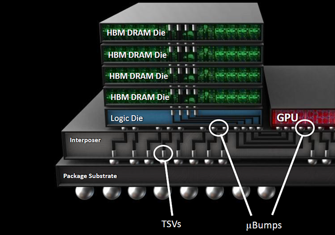
SK Hynix has quietly added its HBM Gen 2 memory stacks to its public product catalog earlier this month, which means that the start of mass production should be imminent. The company will first offer two types of new memory modules with the same capacity, but different transfer-rates, targeting graphics cards, HPC accelerators and other applications. Over time, the HBM2 family will get broader.
SK Hynix intends to initially offer its clients 4 GB HBM2 4Hi stack KGSDs (known good stack dies) based on 8 Gb DRAM devices. The memory devices will feature a 1024-bit bus as well as 1.6 GT/s (H5VR32ESM4H-12C) and 2.0 GT/s (H5VR32ESM4H-20C) data-rates, thus offering 204 GB/s and 256 GB/s peak bandwidth per stack. Earlier this year a representative for SK Hynix revealed plans (in an interview with Golem.de) to start volume production of 4 GB HBM2 KGSDs in Q3 and the addition of the devices into product catalog confirms this information. Keep in mind that memory companies usually make announcements about the start of mass production when they are ready to deliver the first batch of new DRAM to a customer(s). Therefore, it is possible that SK Hynix may already be producing HBM2 stacks.
| Specifications of SK Hynix's HBM2 Memory Chips | ||||||||
| Part Number | Density | Data Rate | Bandwidth per Stack |
Packaging | Feature | Availability | ||
| H5VR32ESM4H-20C | 4 GB | 2.0 GT/s | 256 GB/s | 5mKGSD | 4Hi stack, VDD/VDDQ=1.2V | Q3'16 | ||
| H5VR32ESM4H-12C | 1.6 GT/s | 204 GB/s | ||||||
As outlined in our article published earlier this year, HBM2 memory can stack two, four or eight DRAM devices (2Hi, 4Hi, 8Hi stacks) interconnected using through silicon vias (TSVs) on a base logic die per KGSD (known good stacked die). Each DRAM device features two 128-bit channels, which use DDR signaling with a 2n prefetch architecture (256 bits per memory read and write access) and can operate at their own frequency or even in their own mode. SK Hynix uses 21 nm process technology to make its HBM2 memory and eventually plans to offer 2 GB and 8 GB KGSDs (featuring two or eight 8 Gb DRAM ICs) in addition to 4 GB stacks, aimed at providing memory for various applications. All HBM2 memory products from the company will have 1.2 V VDD/VDDQ and will come in new packages featuring 7.75 mm × 11.87 mm (91.99 mm2) dimensions.
Samsung Electronics began to mass produce its 4 GB 4Hi stack HBM2 KGSDs featuring 2 GT/s data-rate earlier this year and NVIDIA employed the new chips for its GP100 GPU. The first NVIDIA-branded card to use the HBM2 is the Tesla P100 compute accelerator, which has 16 GB of HBM2 memory with 720 GB/s bandwidth (as the DRAM interface operates at about 1.4 GT/s data-rate).

Speaking of HBM2 usage by commercial SoCs, last year SK Hynix said that it worked with 10 companies on various projects (including ASICs, x86 processors, ASSPs and FPGAs) featuring HBM memory (both generations), which indicates that the interest for multi-layer high-bandwidth DRAM is here. However, so far only AMD and NVIDIA have introduced actual products featuring HBM and HBM2.
When it comes to the original HBM, it is worth to mention that SK Hynix has removed such stacks from its catalog. It is unknown whether the company continues to ship them to interested parties, but given the fact that there are not a lot of products that utilize HBM1 today, small scale shipments should not be a problem (at least, until SK Hynix phases out its 29 nm production lines). Meanwhile, since HBM2 is here, it is feasible to assume that we are not going to see many new devices utilizing HBM1.
Source: SK Hynix


43 Comments
View All Comments
ChefJeff789 - Tuesday, August 2, 2016 - link
I actually think this is one of the only ways AMD can make a convincing comeback. I doubt I would consider buying anything else if it was a solid implementation. One chip, one cooling solution. Throw it into a solid motherboard and add an SSD. Nvidia and Intel have nothing to compete with something like that and it could finally force them to compete at the low end. My hope is a ~470 level Polaris on-die with Zen. We'll see next yearhaukionkannel - Tuesday, August 2, 2016 - link
I Also beleive that HBM with zen could be really good for very small htpc computers. It would be slover than Intel in the Office programs, but would be much faster in the games. So when not needed diskrete graphic card, it could be really usefull. Ofcourse bigger Computer with diskrete gpu would be much faster, but what people do with htpc. Look videos, play party games, surf on the web occasionally. Zen with HBM could be perfect for that.Drumsticks - Tuesday, August 2, 2016 - link
That would be one massive CPU die - if AMD made a GPU on the SoC that was fully enabled with 32 CUs (470), it would surely be at least 160mm^2. Add in the CPU die, and HBM, and there'd be something far bigger than what we're used to seeing (in consumer parts). Given the size of AM4, would they actually be able to do that?abufrejoval - Tuesday, August 2, 2016 - link
Is that finally the dawn of a new type of PC?IMHO APUs never made much sense as long as their graphics performance was so limited by the ordinary DDR3/DDR4 DRAM bandwidth (except perhaps if AMD had also been using tile based rendering which parallel discussion around here). And a discrete GPU just made 60% of the die space obsolete and HSA far less efficient.
Putting the GPU on the CPU die is all wrong; you’ve got to do the reverse, adding CPU and the rest of the SoC on the GPU.
The PS/4 chip shows the right path by having all RAM be GDDR5.
HBM2 could make that technically feasible and even economical: At 8GB/stack were talking 32GB per SoC and if that's not enough you'll go SMP/SLI/Stereo for VR or HPC.
And once your die stacking is truly mature, HBM should actually be more economical than ordinary DRAM because you can “outsource” a lot of the amplification work to the base chip.
Perhaps even some logic?
Depending on the level of Integration available on Zen variants I can easily see single die carrier PCs with little more than some PHYs and connectors on the so called motherboard.
Discrete-DRAM-be-dammed the entire "motherboard" would just fit below a nice large and quietly blowing cooler: The NUC would be a Nano!
There could still be variants with PCIe or perhaps just PCIe backplanes for the "motherboard" for those going SMP or wanting to add some odd PCIe add-in, but with a couple of USB 3.1 ports most desktops should be fine.
I guess essentially the desktop PC would have just caught up with the mobile variant but suddenly everything under my desk seems like a dinosaur.
Raniz - Tuesday, August 2, 2016 - link
Main problem with a SoC PC is that you lose the possibility to do partial upgrades. My 5 year old Sandy Bridge i7 can still keep up today and 16GB of RAM is still plenty enough, but that GTX 560 is really weak.An APU with integrated memory would be fairly expensive and you have to replace it completely once it's time to upgrade the graphics card even though the memory and CPU parts of it may still be enough. It's wasteful and costly.
haukionkannel - Tuesday, August 2, 2016 - link
Ofcourse if we talk so big Computer that you can replace parts, it is better to have diskrete gpu, bit if we talk about small hand size computers, then there just is not alternatives.abufrejoval - Tuesday, August 2, 2016 - link
The HBM story is much about flexibility vs. fixed function/allocation.You pay for the flexibility of external DRAM in latency and with lots of extra energy.Ultimately there must be balance between memory capacity and CPU power, GPU power and memory bandwidth. That's why I'd still want to be able to put multiple SoC together to create an SMP system where I want VR and/or higher resolution: It would give more more of everything.
And someone might still take the last gen APU off your hands, should you believe an upgrade is required.
Roland00Address - Tuesday, August 2, 2016 - link
What is the power consumption of HBM2What is the power consumption of HBM2 compared to DDR4? Compared to gddr5?
supdawgwtfd - Tuesday, August 2, 2016 - link
Lower. It's one of the points AMD created it.DanNeely - Tuesday, August 2, 2016 - link
I'm not sure where it stands vs standard DDR; but HBM is significantly more power efficient than GDDR. OTOH each new generation of GPU pushes memory harder and pushes up the power consumption again. IIRC the bars from this nvidia slide represent the ram used with successive generations of GPUs; and while HBM reduced power enough to delay it by a few generations there's still a looming power crisis threatening future generations of GPUs. My suspicion is that the unspecified next generation memory on the AMD slide about the upcoming Navi GPU will probably be an HBM2 successor redesigned to be more power efficient within the memory dies themselves (HBMs savings come from massively reducing data bus power).http://www.3dcenter.org/image/view/9634/_original